SBAA541 December 2022 AMC1202 , AMC1302 , AMC1306M05 , AMC22C11 , AMC22C12 , AMC23C10 , AMC23C11 , AMC23C12 , AMC23C14 , AMC23C15 , AMC3302 , AMC3306M05
- Abstract
- Trademarks
- 1Introduction
-
2Current Sensing in AC/DC Converters
- 2.1 Basic Hardware and Control Description of AC/DC
- 2.2 Point A and B – AC/DC AC Phase-Current Sensing
- 2.3 Point C and D – AC/DC DC Link Current Sensing
- 2.4 Summary of Positives and Negatives at Point A, B, C1/2 and D1/2 and Product Suggestions
- 3Current Sensing in DC/DC Converters
- 4Conclusion
- 5References
3.3 Point G - DC/DC Tank Current Sensing
This section details the current-sensing requirement at the switching tank - point G. In a resonant CLLLC bidirectional isolated DC/ DC converter zero crossing detection (ZCD) is required for synchronous rectification, which helps reducing the conduction loss and improve system efficiency.
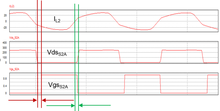
In Figure 3-6, the two green cursor lines indicate the propagation delay between zero crossing and secondary side FET turn-on.
 Figure 3-7 Propagation Delay of Zero Crossing Detection
A state-of-the-art implementation of the ZCD circuit in CLLLC topology is placing a Current Transformer (CT) or a Rogowski coil at the primary and secondary side in series with the resonant capacitor. Typical propagation delays of the CT or Rogowski coil approach are between 100ns and 200ns. This delay can cause significant losses in a CLLLC topology impacting overall efficiency of the DC/DC converter in a negative way. Assuming peak current is about 30 A, the resonate switching frequency of 500 kHz and turn-on delay of 100ns, the body diode (with a forward voltage of 4.5 V) the FET carries 9.3 A until the FET is turned on, which results in a peak energy loss of about 42 W per FET.
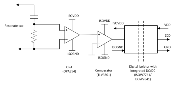
An alternative approach is shown in Figure 3-8. Here, the resonate capacitor voltage in conjunction with a differentiator circuit is implemented to recreate the sinusoidal current. The recreated sinusoidal signal is further processed by a differential-to-single-end OPA(OPA354) and a fast Comparator (TLV3501) for ZCD.
 Figure 3-8 ZCD Circuit With ISOW7741, ISOW7841
The zero-crossing signal is isolated by a digital isolator (ISOW7741 or ISOW7841). These digital isolators have integrated isolated DC/DC converters to generate an isolated supply for the OPA and Comparator devices. The OPA354, TLV3501, and ISOW7741 have propagation delays of 0.6ns, 4.5ns, and 10.7ns, respectively, resulting in a total propagation delay 15.8ns for the complete design, which is about 10 times smaller than a CT or Rogowski coil approach. Assume the same switching frequency and peak current as in the previous example, the peak energy loss in one FET can be reduced from 42 W down to 6.7 W only (impacting overall efficiency positively).