ZHCSBM8C September   2013  – October 2014 DRV8860

PRODUCTION DATA.  

  1. 特性
  2. 应用范围
  3. 说明
  4. 简化电路原理图
  5. 修订历史记录
  6. Pin Configuration and Functions
  7. Specifications
    1. 7.1 Absolute Maximum Ratings
    2. 7.2 Handling Ratings
    3. 7.3 Recommended Operating Conditions
    4. 7.4 Thermal Information
    5. 7.5 Electrical Characteristics
    6. 7.6 Timing Requirements
    7. 7.7 Typical Characteristics
  8. Detailed Description
    1. 8.1 Overview
    2. 8.2 Functional Block Diagram
    3. 8.3 Feature Description
      1. 8.3.1 Recommended Output Current
      2. 8.3.2 Daisy Chain Connection
      3. 8.3.3 Protection Circuits
        1. 8.3.3.1 Overcurrent Protection (OCP)
        2. 8.3.3.2 Open Load Detection (OL)
        3. 8.3.3.3 Thermal Shutdown (TSD)
        4. 8.3.3.4 Undervoltage Lockout (UVLO)
        5. 8.3.3.5 Digital Noise Filter
    4. 8.4 Device Functional Modes
      1. 8.4.1 Internal Registers
    5. 8.5 Programming
      1. 8.5.1 Serial Control Interface
        1. 8.5.1.1 Data Writing Waveform
        2. 8.5.1.2 Fault Register Reading Waveform
        3. 8.5.1.3 Special Command
          1. 8.5.1.3.1 Special command: Write Control Register
          2. 8.5.1.3.2 Special command: Read Control Register
          3. 8.5.1.3.3 Special command: Read Data Register
          4. 8.5.1.3.4 Special command: Fault Register Reset
          5. 8.5.1.3.5 Special command: PWM Start
        4. 8.5.1.4 Output Energizing and PWM Control
          1. 8.5.1.4.1 PWM Start Special Command Used
    6. 8.6 Register Maps
      1. 8.6.1 Data Register
      2. 8.6.2 Fault Register
      3. 8.6.3 Control Register
  9. Application and Implementation
    1. 9.1 Application Information
    2. 9.2 Typical Application
      1. 9.2.1 Design Requirements
      2. 9.2.2 Detailed Design Procedure
        1. 9.2.2.1 Drive Current
      3. 9.2.3 Application Curves
  10. 10Power Supply Recommendations
    1. 10.1 Power Supply and Logic Sequencing
  11. 11Layout
    1. 11.1 Layout Guidelines
    2. 11.2 Layout Example
    3. 11.3 Thermal Consideration
      1. 11.3.1 Power Dissipation
      2. 11.3.2 Heatsinking
  12. 12器件和文档支持
    1. 12.1 商标
    2. 12.2 静电放电警告
    3. 12.3 术语表
  13. 13机械封装和可订购信息

封装选项

机械数据 (封装 | 引脚)
散热焊盘机械数据 (封装 | 引脚)
订购信息

1 特性

  • 8 通道受保护低边驱动器
    • 8 个具有过流保护功能的 NMOS 场效应晶体管 (FET)
    • 集成型感应集流二极管
    • 串行接口
    • 开路/短路负载检测
    • 可配置 100% 占空比输出时间
    • 可配置脉宽调制 (PWM) 占空比
  • 持续电流驱动能力
    • 560 mA(单通道打开)PW 和 PWP
    • 200 mA(八通道打开)PW
    • 330 mA(八通道打开)PWP
    • 支持并联配置
  • 8V 至 38V 电源电压范围
  • 数字输入滤波器
  • 内部数据回读功能
  • 保护和诊断特性
    • 过流保护 (OCP)
    • 开路负载检测 (OL)
    • 过热关断 (OTS)
    • 欠压闭锁 (UVLO)
    • 独立通道状态报告
    • 故障情况警报

2 应用范围

  • 继电器、单极步进电机
  • 螺线管,电磁驱动器
  • 常见低边开关应用

3 说明

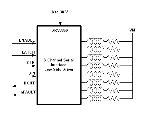
DRV8860 是一款 8 通道低边驱动器,此驱动器具有过流保护和开路/短路负载检测功能。 它具有内置的用来钳制由电感负载生成的关闭瞬态的二极管,可被用于驱动单极步进电机、直流电机、继电器、螺线管、或者其它负载。

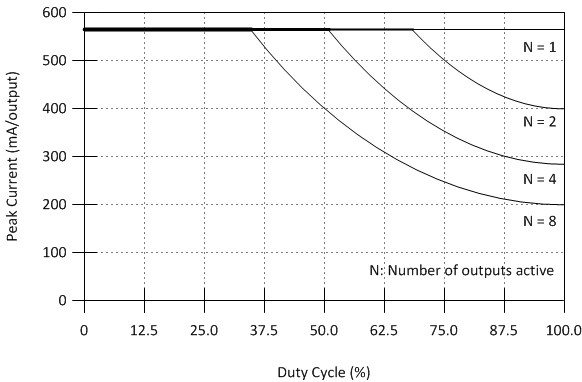
DRV8860PWP 可提供最高 330mA(8 通道打开)的连续输出电流,DRV8860PW 则可提供最高 200mA(8 通道打开)的连续输出电流。 此电流驱动能力随着 PWM 占空比的降低而增加。 单一通道打开时能够驱动高达 560mA 的持续输出电流。 细节请参考部分。输出电流建议

提供了一个串口来控制 DRV8860 输出驱动器、配置内部设置寄存器以及读取每条通道的故障状态。 多个 DRV8860 器件可采用菊花链连在一起以共同使用一个单一串口。 也可通过串口来配置加电时间和保持 PWM 占空比。 利用这些功能,可实现比传统的始终开启解决方案更低的运行温度。

还提供用于过流保护、短路保护、欠压闭锁和过热保护的内部关断功能。 DRV8860 能够诊断开路负载情况。 每条通道的故障信息可由串口读取,并且有一个外部故障引脚指示。

器件信息(1)

部件号 封装 封装尺寸(标称值)
DRV8860 TSSOP (16) 5.00mm x 6.40mm
HTSSOP (16)
  1. 要了解所有可用封装,请见数据表末尾的可订购产品附录。

4 简化电路原理图

Simplified_schematic_slar065.gif
FPGraph_slrs065.gif