SGLS386F January 2009 – October 2014 DAC5670-SP
PRODUCTION DATA.
- 1 Features
- 2 Applications
- 3 Description
- 4 Revision History
- 5 Description (continued)
- 6 Pin Configuration and Functions
- 7 Specifications
- 8 Detailed Description
- 9 Application and Implementation
- 10Power Supply Recommendations
- 11Layout
- 12Device and Documentation Support
- 13Mechanical, Packaging, and Orderable Information
1 Features
- 14-Bit Resolution
- 2.4-GSPS Max Update Rate DAC
- Dual Differential Input Ports
- Even/Odd Demultiplexed Data
- Maximum 1.2 GSPS Each Port, 2.4 GSPS Total
- Dual 14-Bit Inputs + 1 Reference Bit
- DDR Output Clock
- DLL Optimized Clock Timing Synchronized to Reference Bit
- LVDS and HyperTransport™ Voltage Level Compatible
- Internal 100-Ω Terminations for Data and Reference Bit Inputs
- Selectable 2× Interpolation With Fs / 2 Mixing
- Differential Scalable Current Outputs: 5 to 30 mA
- On-Chip 1.2-V Reference
- 3.3-V Analog Supply Operation
- Power Dissipation: 2 W
- 192-Ball CBGA (GEM) Package
- QML-V Qualified, SMD 5962-07247
- Military Temperature Range (–55°C to 125°C Tcase)
2 Applications
- Test and Measurement: Arbitrary Waveform Generator
- Communications
- Engineering evaluation (/EM) samples are available (1)
3 Description
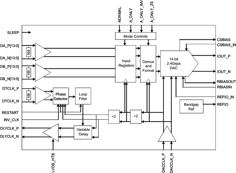
The DAC5670 is a 14-bit 2.4-GSPS DAC with dual demultiplexed differential input ports. The DAC5670 is clocked at the DAC sample rate and the two input ports run at a maximum of 1.2 GSPS. An additional reference bit input sequence is used to adjust the output clock delay to the data source, optimizing the internal data latching clock relative to this reference bit with a delay lock loop (DLL). Alternatively, the DLL may be bypassed and the timing interface managed by controlling DATA setup and hold timing to DLYCLK.
The DAC5670 can also accept data up to 1.2 GSPS using only the A input port. In the single port modes, options include: repeating the input sample (A_ONLY mode), 2× interpolation by zero stuff (A_ONLY_ZS mode), or 2× interpolation by repeating and inverting the input sample (A_ONLY_INV). These modes are used to double the input sample rate up to 2.4 GSPS.
The DAC5670 operates with a single 3- to 3.6-V supply voltage. Power dissipation is 2 W at maximum operating conditions. The DAC5670 provides a nominal full-scale differential current-output of 20 mA, supporting both single-ended and differential applications. An on-chip 1.2-V temperature-compensated bandgap reference and control amplifier allows the user to adjust the full-scale output current from the nominal 20 mA to as low as 5 mA or as high as 30 mA.
Device Information(1)
| PART NUMBER | PACKAGE | BODY SIZE (NOM) |
|---|---|---|
| DAC5670-SP | CBGA (192) | 19.00 mm × 19.00 mm |
- For all available packages, see the orderable addendum at the end of the data sheet.
Simplified Schematic
4 Revision History
Changes from E Revision (December 2013) to F Revision
- Added Handling Ratings table, Feature Description section, Device Functional Modes, Application and Implementation section, Power Supply Recommendations section, Layout section, Device and Documentation Support section, and Mechanical, Packaging, and Orderable Information section Go
- Corrected Setup/Hold Data to DLYCLK values to be frequency independentGo
- Updated DLL Usage sectionGo
Changes from D Revision (May 2013) to E Revision