ZHCS501F November 2011 – December 2014 UCC27210 , UCC27211
PRODUCTION DATA.
- 1 特性
- 2 应用
- 3 说明
- 4 修订历史记录
- 5 说明 (续)
- 6 Pin Configuration and Functions
-
7 Specifications
- 7.1 Absolute Maximum Ratings
- 7.2 ESD Ratings
- 7.3 Recommended Operating Conditions
- 7.4 Thermal Information
- 7.5 Electrical Characteristics
- 7.6 Switching Characteristics: Propagation Delays
- 7.7 Switching Characteristics: Delay Matching
- 7.8 Switching Characteristics: Output Rise and Fall Time
- 7.9 Switching Characteristics: Miscellaneous
- 7.10 Typical Characteristics
- 8 Detailed Description
- 9 Application and Implementation
- 10Power Supply Recommendations
- 11Layout
- 12器件和文档支持
- 13机械、封装和可订购信息
封装选项
请参考 PDF 数据表获取器件具体的封装图。
机械数据 (封装 | 引脚)
- D|8
- DRM|8
- DPR|10
- DDA|8
散热焊盘机械数据 (封装 | 引脚)
- DDA|8
订购信息
7 Specifications
7.1 Absolute Maximum Ratings(1)
over operating free-air temperature range (unless otherwise noted)| MIN | MAX | UNIT | ||
|---|---|---|---|---|
| Supply voltage range, VDD(2), VHB - VHS | –0.3 | 20 | V | |
| Input voltages on LI and HI, VLI, VHI | –10 | 20 | ||
| Output voltage on LO, VLO | DC | –0.3 | VDD + 0.3 | |
| Repetitive pulse <100 ns(3) | –2 | VDD + 0.3 | ||
| Output voltage on HO, VHO | DC | VHS – 0.3 | VHB + 0.3 | |
| Repetitive pulse <100 ns(3) | VHS – 2 | VHB + 0.3 | ||
| Voltage on HS, VHS | DC | –1 | 115 | |
| Repetitive pulse <100 ns(3) | –(24 V-VDD) | 115 | ||
| Voltage on HB, VHB | –0.3 | 120 | ||
| Operating virtual junction temperature, TJ | –40 | 150 | °C | |
| Lead temperature (soldering, 10 sec.) | 300 | |||
| Storage temperature, Tstg | –65 | 150 | °C | |
(1) Stresses beyond those listed under Absolute Maximum Ratings may cause permanent damage to the device. These are stress ratings only, and functional operation of the device at these or any other conditions beyond those indicated under Recommended Operating Conditions is not implied. Exposure to absolute-maximum-rated conditions for extended periods may affect device reliability.
(2) All voltages are with respect to VSS unless otherwise noted. Currents are positive into, negative out of the specified terminal.
7.2 ESD Ratings
| VALUE | UNIT | |||
|---|---|---|---|---|
| V(ESD) | Electrostatic discharge | Human body model (HBM), per ANSI/ESDA/JEDEC JS-001(1) | ±2000 | V |
| Charged-device model (CDM), per JEDEC specification JESD22-C101(2) | ±1000 | |||
(1) JEDEC document JEP155 states that 500-V HBM allows safe manufacturing with a standard ESD control process.
(2) JEDEC document JEP157 states that 250-V CDM allows safe manufacturing with a standard ESD control process.
7.3 Recommended Operating Conditions
all voltages are with respect to VSS; currents are positive into and negative out of the specified terminal. –40°C < TJ = TA < 140°C (unless otherwise noted)7.4 Thermal Information
| THERMAL METRIC | UCC27210, UCC27211 | UNIT | ||||
|---|---|---|---|---|---|---|
| D | DDA | DRM | DPR | |||
| 8 PINS | 8 PINS | 8 PINS | 10 PINS | |||
| θJA | Junction-to-ambient thermal resistance(1) | 111.8 | 37.7 | 33.9 | 36.8 | °C/W |
| θJCtop | Junction-to-case (top) thermal resistance(2) | 56.9 | 47.2 | 33.2 | 36.0 | |
| θJB | Junction-to-board thermal resistance(3) | 53.0 | 9.6 | 11.4 | 14.0 | |
| ψJT | Junction-to-top characterization parameter(4) | 7.8 | 2.8 | 0.4 | 0.3 | |
| ψJB | Junction-to-board characterization parameter(5) | 52.3 | 9.4 | 11.7 | 14.2 | |
| θJCbot | Junction-to-case (bottom) thermal resistance(6) | n/a | 3.6 | 2.3 | 3.4 | |
(1) The junction-to-ambient thermal resistance under natural convection is obtained in a simulation on a JEDEC-standard, high-K board, as specified in JESD51-7, in an environment described in JESD51-2a.
(2) The junction-to-case (top) thermal resistance is obtained by simulating a cold plate test on the package top. No specific JEDEC-standard test exists, but a close description can be found in the ANSI SEMI standard G30-88.
(3) The junction-to-board thermal resistance is obtained by simulating in an environment with a ring cold plate fixture to control the PCB temperature, as described in JESD51-8.
(4) The junction-to-top characterization parameter, ψJT, estimates the junction temperature of a device in a real system and is extracted from the simulation data for obtaining RθJA, using a procedure described in JESD51-2a (sections 6 and 7).
(5) The junction-to-board characterization parameter, ψJB, estimates the junction temperature of a device in a real system and is extracted from the simulation data for obtaining RθJA, using a procedure described in JESD51-2a (sections 6 and 7).
(6) The junction-to-case (bottom) thermal resistance is obtained by simulating a cold plate test on the exposed (power) pad. No specific JEDEC standard test exists, but a close description can be found in the ANSI SEMI standard G30-88.
Spacer
Spacer
7.5 Electrical Characteristics
VDD = VHB = 12 V, VHS = VSS = 0 V, no load on LO or HO, TA = TJ = –40°C to 140°C, (unless otherwise noted)| PARAMETER | TEST CONDITIONS | MIN | TYP | MAX | UNIT | ||
|---|---|---|---|---|---|---|---|
| SUPPLY CURRENTS | |||||||
| IDD | VDD quiescent current | V(LI) = V(HI) = 0 V | 0.05 | 0.085 | 0.17 | mA | |
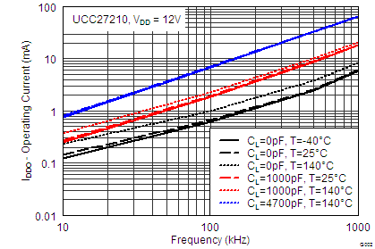
| IDDO | VDD operating current | UCC27210 | f = 500 kHz, CLOAD = 0 | 2.6 | 5.2 | ||
| UCC27211 | 2.5 | 5.2 | |||||
| IHB | Boot voltage quiescent current | V(LI) = V(HI) = 0 V | 0.015 | 0.065 | 0.1 | ||
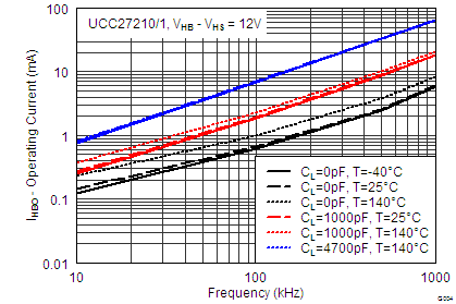
| IHBO | Boot voltage operating current | f = 500 kHz, CLOAD = 0 | 2.5 | 5.0 | |||
| IHBS | HB to VSS quiescent current | V(HS) = V(HB) = 115 V | 0.0005 | 1.0 | µA | ||
| IHBSO | HB to VSS operating current | f = 500 kHz, CLOAD = 0 | 0.07 | 1.2 | mA | ||
| INPUT | |||||||
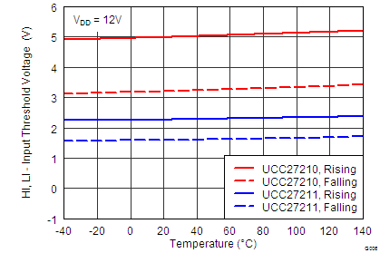
| VHIT | Input voltage threshold | UCC27210 | 4.2 | 5.0 | 5.8 | V | |
| UCC27210 (DDA only) | 4.2 | 5.0 | 5.9 | ||||
| VLIT | Input voltage threshold | UCC27210 | 2.4 | 3.2 | 4.0 | ||
| UCC27210 (DDA only) | 2.4 | 3.2 | 4.0 | ||||
| VIHYS | Input voltage hysteresis | UCC27210 | 1.8 | ||||
| RIN | Input pulldown resistance | 102 | kΩ | ||||
| VHIT | Input voltage threshold | UCC27211 | 1.9 | 2.3 | 2.7 | V | |
| UCC27211 (DDA only) | 1.9 | 2.3 | 2.8 | ||||
| VLIT | Input voltage threshold | UCC27211 | 1.3 | 1.6 | 1.9 | ||
| UCC27211 (DDA only) | 1.3 | 1.6 | 2.1 | ||||
| VIHYS | Input voltage hysteresis | UCC27211 | 700 | mV | |||
| RIN | Input pulldown resistance | 68 | kΩ | ||||
| UNDERVOLTAGE LOCKOUT (UVLO) | |||||||
| VDDR | VDD turnon threshold | 6.2 | 7.0 | 7.8 | V | ||
| DDA only | 5.8 | 7.0 | 8.1 | ||||
| VDDHYS | Hysteresis | 0.5 | |||||
| VHBR | VHB turnon threshold | 5.6 | 6.7 | 7.9 | |||
| DDA only | 5.3 | 6.7 | 8.0 | ||||
| VHBHYS | Hysteresis | 1.1 | |||||
| BOOTSTRAP DIODE | |||||||
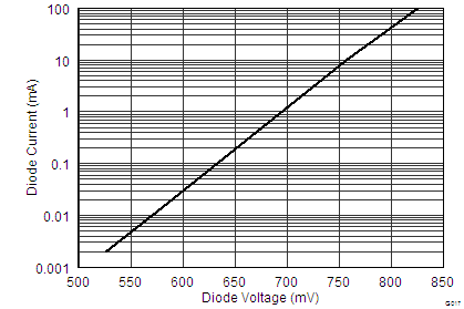
| VF | Low-current forward voltage | IVDD-HB = 100 µA | 0.65 | 0.8 | V | ||
| VFI | High-current forward voltage | IVDD-HB = 100 mA | 0.85 | 0.95 | |||
| RD | Dynamic resistance, ΔVF/ΔI | IVDD-HB = 100 mA and 80 mA | 0.3 | 0.5 | 0.85 | Ω | |
| LO GATE DRIVER | |||||||
| VLOL | Low-level output voltage | ILO = 100 mA | 0.05 | 0.09 | 0.19 | V | |
| VLOH | High level output voltage | ILO = -100 mA, VLOH = VDD - VLO | 0.1 | 0.16 | 0.29 | ||
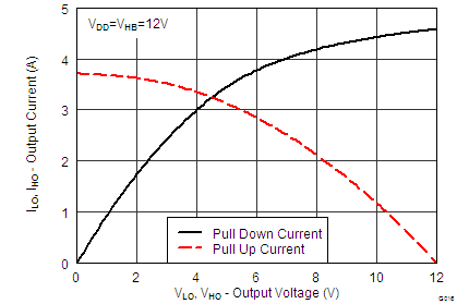
| Peak pull-up current(3) | VLO = 0 V | 3.7 | A | ||||
| Peak pull-down current(3) | VLO = 12 V | 4.5 | |||||
| HO GATE DRIVER | |||||||
| VHOL | Low-level output voltage | IHO = 100 mA | 0.05 | 0.09 | 0.19 | V | |
| VHOH | High-level output voltage | IHO = -100 mA, VHOH = VHB - VHO | 0.1 | 0.16 | 0.29 | ||
| Peak pull-up current(3) | VHO = 0 V | 3.7 | A | ||||
| Peak pull-down current(3) | VHO = 12 V | 4.5 | |||||
(1) Typical values for TA = 25°C.
(2) IF: Forward current applied to bootstrap diode, IREV: Reverse current applied to bootstrap diode.
(3) Ensured by design.
7.6 Switching Characteristics: Propagation Delays
over operating free-air temperature range (unless otherwise noted)7.7 Switching Characteristics: Delay Matching
over operating free-air temperature range (unless otherwise noted)7.8 Switching Characteristics: Output Rise and Fall Time
over operating free-air temperature range (unless otherwise noted)7.9 Switching Characteristics: Miscellaneous
over operating free-air temperature range (unless otherwise noted)| PARAMETER | TEST CONDITIONS | MIN | TYP | MAX | UNIT | |
|---|---|---|---|---|---|---|
| Minimum input pulse width that changes the output | 50 | ns | ||||
| Bootstrap diode turnoff time(3)(2) | IF = 20 mA, IREV = 0.5 A(1) | 20 | ||||
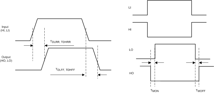 Figure 1. Timing Diagrams
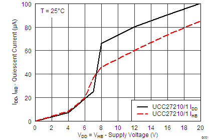
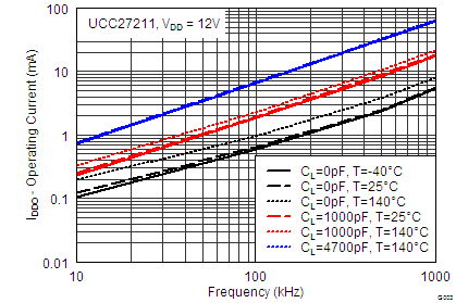
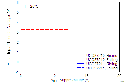
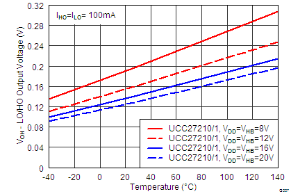
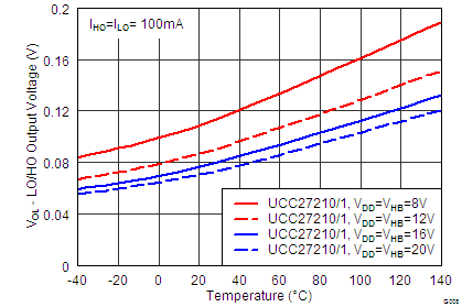
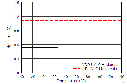
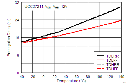
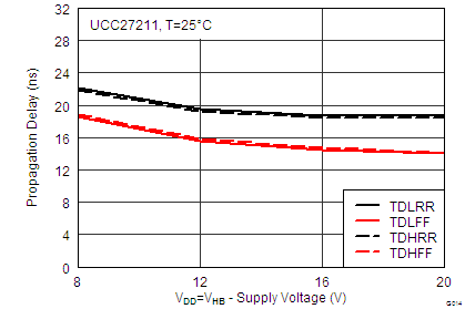
7.10 Typical Characteristics
