ZHCSOE5B March 2022 – January 2023 UCC21737-Q1
PRODUCTION DATA
- 1 特性
- 2 应用
- 3 说明
- 4 Revision History
- 5 Pin Configuration and Functions
-
6 Specifications
- 6.1 Absolute Maximum Ratings
- 6.2 ESD Ratings
- 6.3 Recommended Operating Conditions
- 6.4 Thermal Information
- 6.5 Power Ratings
- 6.6 Insulation Specifications
- 6.7 Safety Limiting Values
- 6.8 Electrical Characteristics
- 6.9 Switching Characteristics
- 6.10 Insulation Characteristics Curves
- 6.11 Typical Characteristics
- 7 Parameter Measurement Information
-
8 Detailed Description
- 8.1 Overview
- 8.2 Functional Block Diagram
- 8.3
Feature Description
- 8.3.1 Power Supply
- 8.3.2 Driver Stage
- 8.3.3 VCC, VDD, and VEE Undervoltage Lockout (UVLO)
- 8.3.4 Active Pulldown
- 8.3.5 Short Circuit Clamping
- 8.3.6 External Active Miller Clamp
- 8.3.7 Overcurrent and Short Circuit Protection
- 8.3.8 Soft Turn-off
- 8.3.9 Fault (FLT), Reset, and Enable (RST/EN)
- 8.3.10 ASC Support and APWM Monitor
- 8.4 Device Functional Modes
-
9 Applications and Implementation
- 9.1 Application Information
- 9.2
Typical Application
- 9.2.1 Design Requirements
- 9.2.2
Detailed Design Procedure
- 9.2.2.1 Input Filters for IN+, IN-, and RST/EN
- 9.2.2.2 PWM Interlock of IN+ and IN-
- 9.2.2.3 FLT, RDY, and RST/EN Pin Circuitry
- 9.2.2.4 RST/EN Pin Control
- 9.2.2.5 Turnon and Turnoff Gate Resistors
- 9.2.2.6 External Active Miller Clamp
- 9.2.2.7 Overcurrent and Short Circuit Protection
- 9.2.2.8 Higher Output Current Using an External Current Buffer
- 9.2.3 Application Curves
- 10Power Supply Recommendations
- 11Layout
- 12Device and Documentation Support
- 13Mechanical, Packaging, and Orderable Information
6.11 Typical Characteristics
| VDD = 20 V, VEE = –5 V |
| VDD = 20 V, VEE = –5 V |
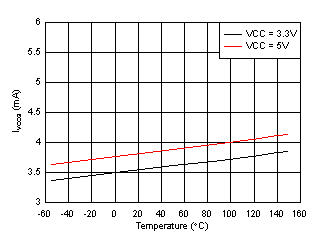
| IN+ = High | IN- = Low |
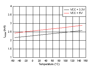
| IN+ = Low | IN- = Low |
Figure 6-8 IVCCQ Supply Current vs Input Frequency
| VDD = 20 V, VEE = –5 V | IN+ = High, IN- = Low |
| VDD = 20 V, VEE = –5 V | IN+ = Low, IN- = Low |
| VDD/VEE = 20 V/–5 V |
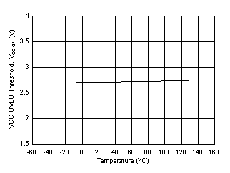 Figure 6-12 VCC UVLO vs
Temperature
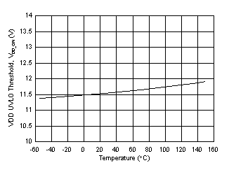 Figure 6-13 VDD UVLO vs
Temperature
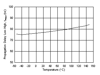
| VCC = 3.3 V | VDD = 18 V | CL = 100 pF |
| RON = 0 Ω | ROFF = 0 Ω |
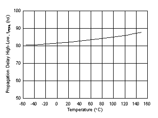
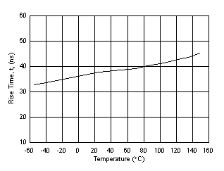
| VCC = 3.3 V | VDD = 18 V | CL = 100 pF |
| RON = 0 Ω | ROFF = 0 Ω |
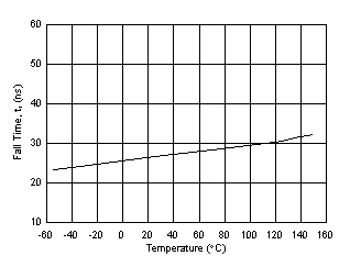
| VCC = 3.3 V | VDD = 18 V | CL = 10 nF |
| RON = 0 Ω | ROFF = 0 Ω |
| VCC = 3.3 V | VDD = 18 V | CL = 10 nF |
| RON = 0 Ω | ROFF = 0 Ω |
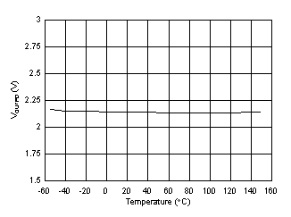 Figure 6-18 VOUTPD Output
Active Pulldown Voltage vs Temperature
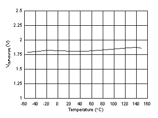
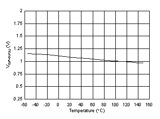
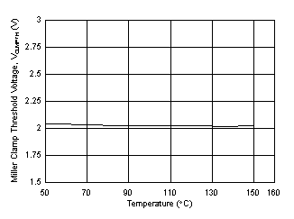 Figure 6-21 VCLMPTH Miller
Clamp Threshold Voltage vs Temperature