ZHCSIF5F December 2015 – April 2019 TPS99000-Q1
PRODUCTION DATA.
- 1 特性
- 2 应用
- 3 说明
- 4 修订历史记录
- 5 Pin Configuration and Functions
-
6 Specifications
- 6.1 Absolute Maximum Ratings
- 6.2 ESD Ratings
- 6.3 Recommended Operating Conditions
- 6.4 Thermal Information
- 6.5 Electrical Characteristics - Transimpedance Amplifier Parameters
- 6.6 Electrical Characteristics - Digital to Analog Converters
- 6.7 Electrical Characteristics - Analog to Digital Converter
- 6.8 Electrical Characteristics - FET Gate Drivers
- 6.9 Electrical Characteristics - Photo Comparator
- 6.10 Electrical Characteristics - Voltage Regulators
- 6.11 Electrical Characteristics - Temperature and Voltage Monitors
- 6.12 Electrical Characteristics - Current Consumption
- 6.13 Power-Up Timing Requirements
- 6.14 Power-Down Timing Requirements
- 6.15 Timing Requirements - Sequencer Clock
- 6.16 Timing Requirements - Host / Diagnostic Port SPI Interface
- 6.17 Timing Requirements - ADC Interface
- 6.18 Switching Characteristics
-
7 Detailed Description
- 7.1 Overview
- 7.2 Functional Block Diagram
- 7.3
Feature Description
- 7.3.1
Illumination Control
- 7.3.1.1 Illumination System High Dynamic Range Dimming Overview
- 7.3.1.2 Illumination Control Loop
- 7.3.1.3 Continuous Mode Operation
- 7.3.1.4
Discontinuous Mode Operation
- 7.3.1.4.1 Discontinuous Mode Pulse Width Limit
- 7.3.1.4.2 COMPOUT_LOW Timer in Discontinuous Operation
- 7.3.1.4.3 Dimming Within Discontinuous Operation Range
- 7.3.1.4.4 Multiple Pulse Heights to Increase Bit Depth
- 7.3.1.4.5 TIA Gain Adjustment
- 7.3.1.4.6 Current Limit in Discontinuous Mode
- 7.3.1.4.7 CMODE Big Cap Mode in Discontinuous Operation
- 7.3.2 Over-Brightness Detection
- 7.3.3 Analog to Digital Converter
- 7.3.4 Power Sequencing and Monitoring
- 7.3.5 DMD Mirror Voltage Regulator
- 7.3.6 Low Dropout Regulators
- 7.3.7 System Monitoring Features
- 7.3.8 Communication Ports
- 7.3.1
Illumination Control
- 7.4 Device Functional Modes
- 7.5 Register Maps
- 8 Application and Implementation
- 9 Power Supply Recommendations
- 10Layout
- 11器件和文档支持
- 12机械、封装和可订购信息
封装选项
机械数据 (封装 | 引脚)
- PZP|100
散热焊盘机械数据 (封装 | 引脚)
- PZP|100
订购信息
9.3 Power Supply Architecture
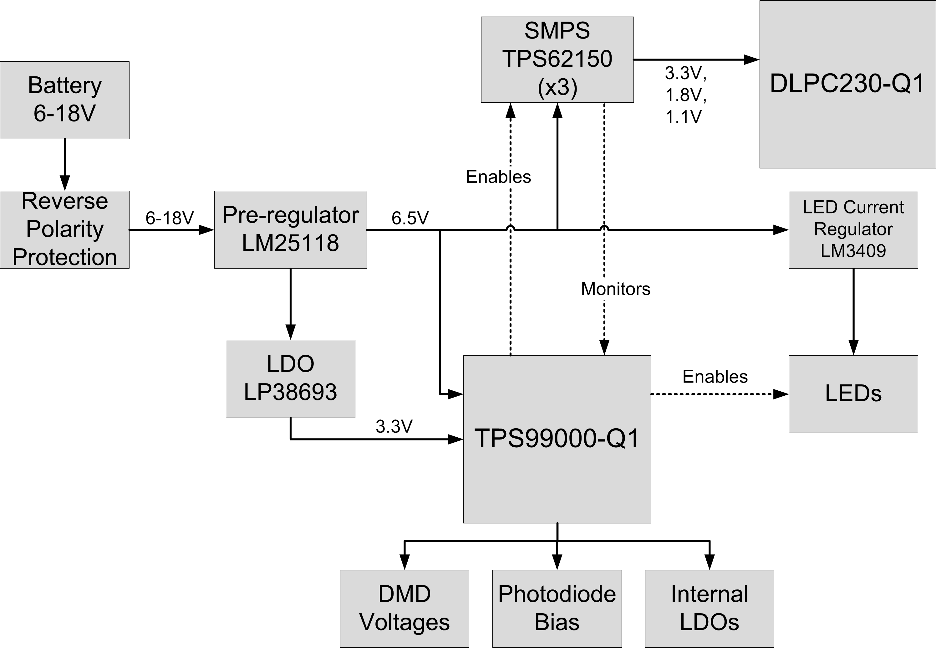
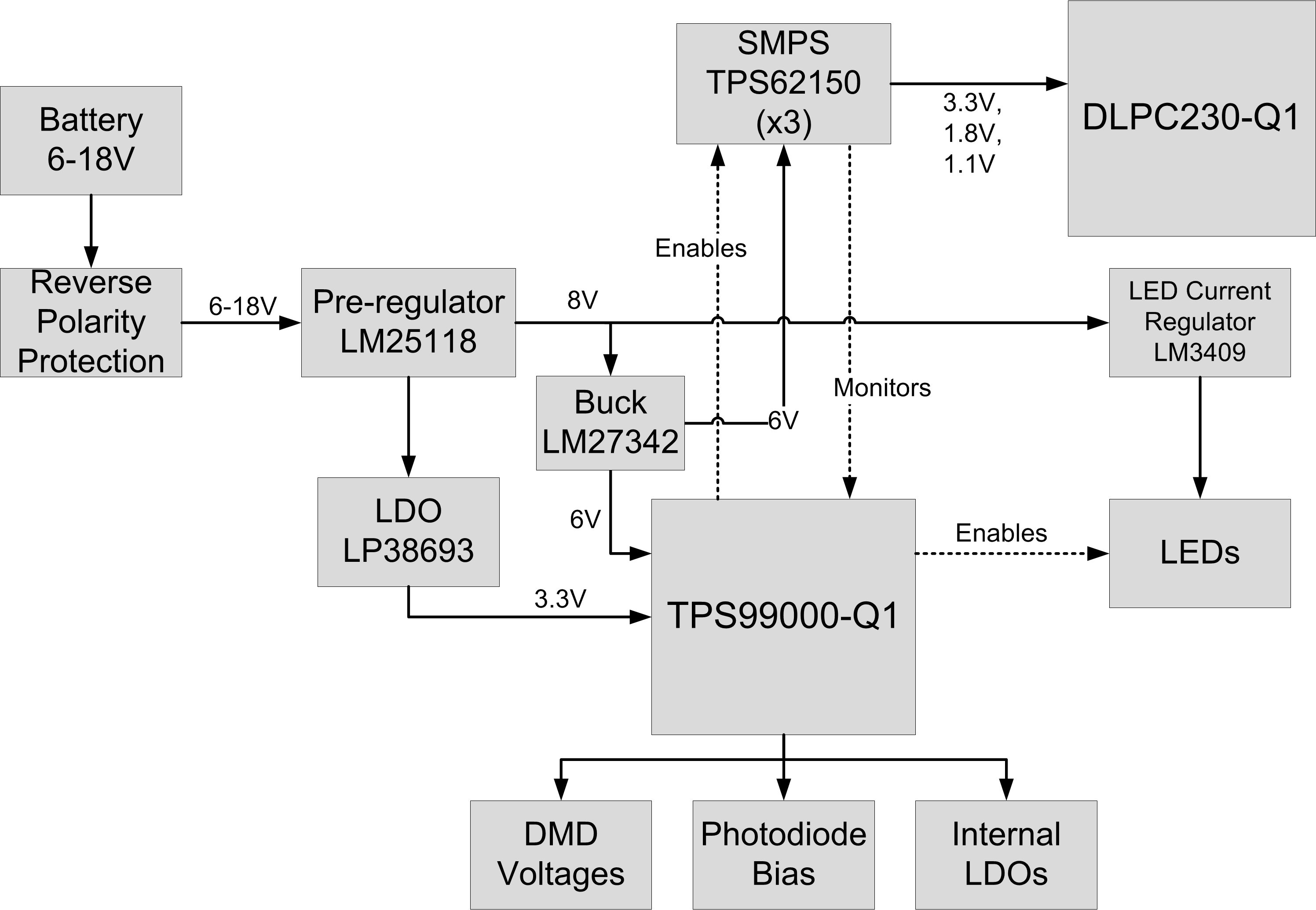
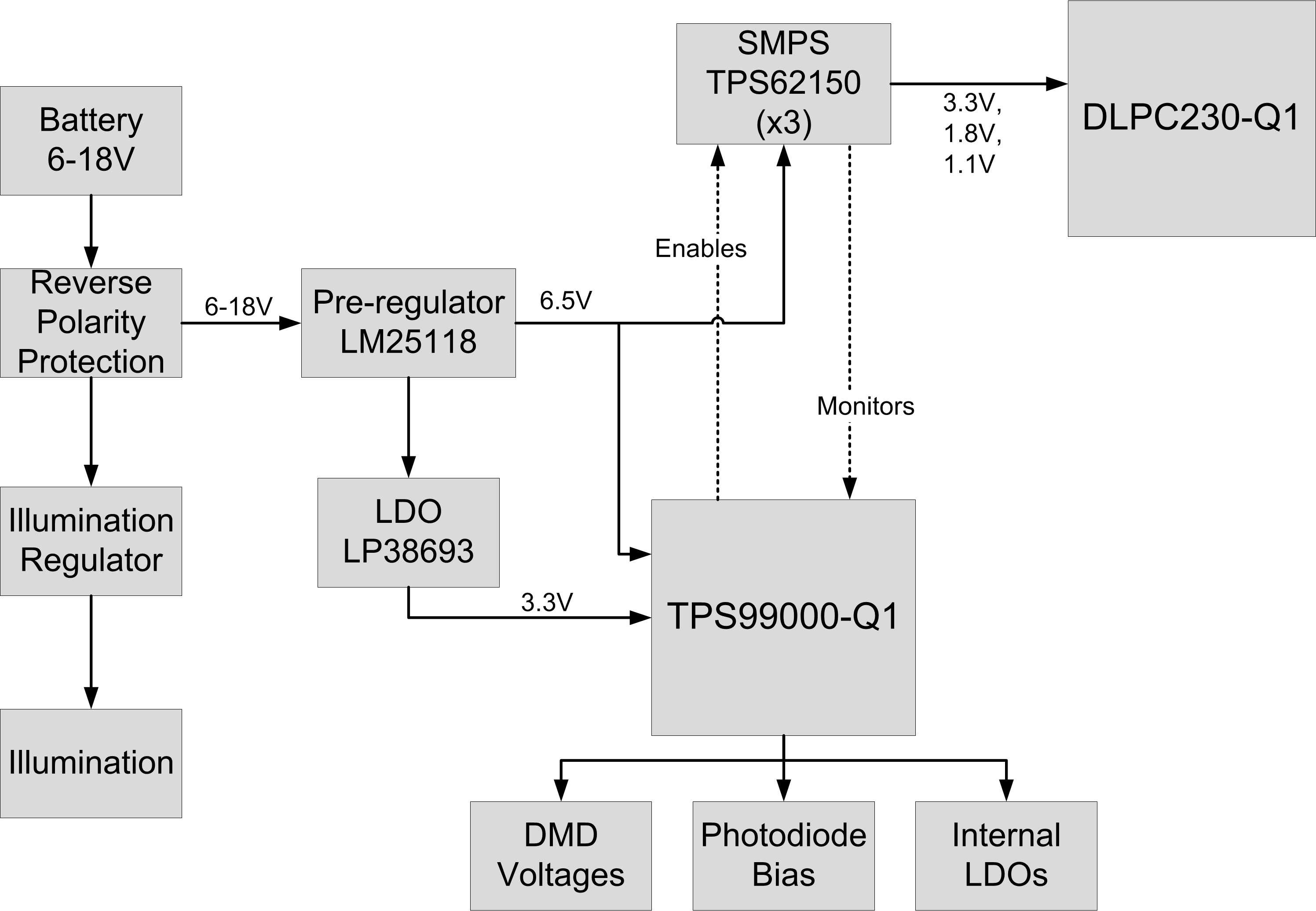
The power supply architecture depends on the amount of power required for the illumination source. For HUD applications which require precise color and white point control, it is highly recommended to pre-regulate the illumination power supply, as voltage variations can cause variations in the LED output. For non-color critical applications, the designer may choose to completely isolate the illumination driver. In addition, if 2 or more LEDs are driven in series, then the pre-regulated voltage must be higher than the voltage of the LEDs. The different architectures are shown below.
Note that the architectures make use of the LM25118 as a pre-regulator. This part uses a buck-boost architecture which allows it to supply the required 6.5 V with a battery voltage input of 6 V to 18 V. If the battery input can be assured to be above the 6.5 V output voltage, then a buck architecture can be used instead, resulting in BOM savings.
 Figure 48. Architecture Number 1: HUD Application with LED Forward Voltage Less Than 5 V
 In this application, the same pre-regulator is used to power the 6.5 V rail as well as the LM3409. Since the LM3409 input voltage must be kept above 6 V, the pre-regulator is set to 6.5 V.
 Figure 49. Architecture Number 2: HUD Application with Two LEDs in Series Configuration
 In this application, the pre-regulator must be designed to operate at a higher output voltage in order to drive 2 LEDs in series. Because the TPS99000-Q1 requires a VIN from 5.5 V to 7 V, a small buck regulator is used to generate a 6 V power rail.
 Figure 50. Architecture Number 3: Headlight Application with Independent Illumination
 In this application, the power used to drive the illumination is separate from the TPS99000-Q1. This is possible in applications where the illumination driver can be very simple. Although the LM25118 is shown here, a different regulator would likely be selected in this application because the maximum current requirements are much less with the illumination power path removed.