ZHCSIF5F December 2015 – April 2019 TPS99000-Q1
PRODUCTION DATA.
- 1 特性
- 2 应用
- 3 说明
- 4 修订历史记录
- 5 Pin Configuration and Functions
-
6 Specifications
- 6.1 Absolute Maximum Ratings
- 6.2 ESD Ratings
- 6.3 Recommended Operating Conditions
- 6.4 Thermal Information
- 6.5 Electrical Characteristics - Transimpedance Amplifier Parameters
- 6.6 Electrical Characteristics - Digital to Analog Converters
- 6.7 Electrical Characteristics - Analog to Digital Converter
- 6.8 Electrical Characteristics - FET Gate Drivers
- 6.9 Electrical Characteristics - Photo Comparator
- 6.10 Electrical Characteristics - Voltage Regulators
- 6.11 Electrical Characteristics - Temperature and Voltage Monitors
- 6.12 Electrical Characteristics - Current Consumption
- 6.13 Power-Up Timing Requirements
- 6.14 Power-Down Timing Requirements
- 6.15 Timing Requirements - Sequencer Clock
- 6.16 Timing Requirements - Host / Diagnostic Port SPI Interface
- 6.17 Timing Requirements - ADC Interface
- 6.18 Switching Characteristics
-
7 Detailed Description
- 7.1 Overview
- 7.2 Functional Block Diagram
- 7.3
Feature Description
- 7.3.1
Illumination Control
- 7.3.1.1 Illumination System High Dynamic Range Dimming Overview
- 7.3.1.2 Illumination Control Loop
- 7.3.1.3 Continuous Mode Operation
- 7.3.1.4
Discontinuous Mode Operation
- 7.3.1.4.1 Discontinuous Mode Pulse Width Limit
- 7.3.1.4.2 COMPOUT_LOW Timer in Discontinuous Operation
- 7.3.1.4.3 Dimming Within Discontinuous Operation Range
- 7.3.1.4.4 Multiple Pulse Heights to Increase Bit Depth
- 7.3.1.4.5 TIA Gain Adjustment
- 7.3.1.4.6 Current Limit in Discontinuous Mode
- 7.3.1.4.7 CMODE Big Cap Mode in Discontinuous Operation
- 7.3.2 Over-Brightness Detection
- 7.3.3 Analog to Digital Converter
- 7.3.4 Power Sequencing and Monitoring
- 7.3.5 DMD Mirror Voltage Regulator
- 7.3.6 Low Dropout Regulators
- 7.3.7 System Monitoring Features
- 7.3.8 Communication Ports
- 7.3.1
Illumination Control
- 7.4 Device Functional Modes
- 7.5 Register Maps
- 8 Application and Implementation
- 9 Power Supply Recommendations
- 10Layout
- 11器件和文档支持
- 12机械、封装和可订购信息
封装选项
机械数据 (封装 | 引脚)
- PZP|100
散热焊盘机械数据 (封装 | 引脚)
- PZP|100
订购信息
8.2.1.2.6 Transimpedance Amplifiers (TIAs, Usage, Offset, Dark Current, Ranges, RGB Trim)
The TPS99000-Q1 includes support for up to 2 system photodiode inputs.
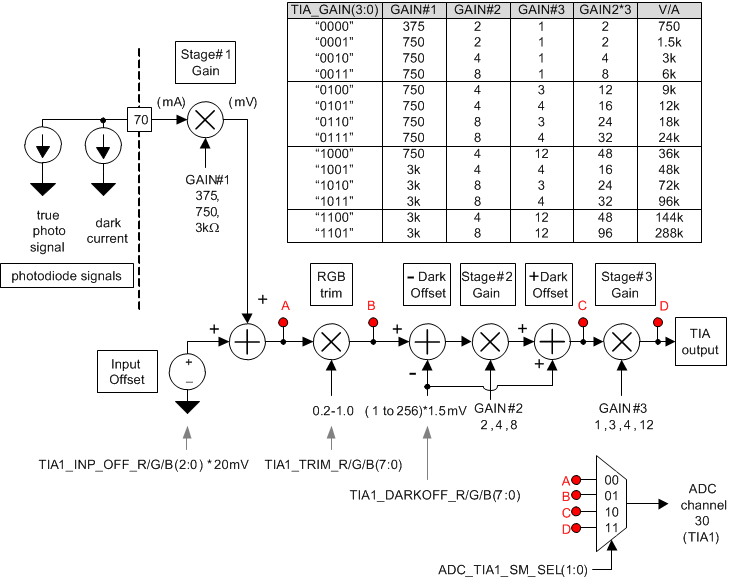
TIA1 is used as the primary photo feedback channel. It supports 14 unique gain settings, spanning 0.75 kV/A to 288 kV/A. In addition, these gain settings can be adjusted downward by a high resolution trim function, in a range of 1.0x to 0.2x. This trim function has independent RGB settings, supporting color rebalancing (such as trimming RGB feedback signals so that white light produces roughly equal voltages at TIA output for each color). Color rebalancing helps keep all three color channels in the working voltage range to maximize dynamic range. Figure 46 shows the TIA1 model.
 Figure 46. TIA1 Trim, Offset, and Gain Stages
 TIA2 supports a single trim value and single darkoffset value, but is otherwise identical to TIA1.
NOTE
TIA2 shall only be used for diagnostic purposes, and it is not recommended to use for primary photo feedback amplification. If TIA2 is used to measure projector output or illumination light, this lack of multiplexed RGB parameters for trim and dark offset will limit its usage to looking only at one color at a time for situations where highest gain settings are used in combination with high color to color electrical response imbalance. For lower gain settings or situations where the photodiode responses are naturally balanced, all 3 colors likely can be monitored with TIA2.
The trim settings may be used to lower the total gain of the TIA amplifiers. This provides flexibility to allow higher photo diode currents to be used without saturating the TIA. For example, with the trim setting limited to 0.5×, a 0.75-kV/A gain selection can be considered a 0.375-kV/A effective gain setting. The supported maximum photo diode current doubles in this case.
Both TIAs are designed to support a wide range of photo diode capacitances. A variable, internal compensation capacitor network is available to tune the circuit for maximum performance for a given photo diode and cable combination.
Both TIAs can be independently enabled or disabled. When a TIA is disabled, it is placed in a low power mode to optimize power consumption.
TIA2 can be used for an over-brightness detection input or ADC measurements. It supports two outputs: 1) a higher bandwidth output, optimized for measuring photo diode response of CM bit slice light pulses, and 2) a much lower bandwidth output, optimized for measuring light flux filter over periods spanning at least one video frame. TIA1 supports these same two outputs, plus one more: a very high bandwidth output used for the real-time color control loop photo feedback. See Electrical Characteristics - Transimpedance Amplifier Parameters for BW and slew rate specifications for this use case.
One potential use for TIA2 is for system level brightness detection.