ZHCSIF5F December 2015 – April 2019 TPS99000-Q1
PRODUCTION DATA.
- 1 特性
- 2 应用
- 3 说明
- 4 修订历史记录
- 5 Pin Configuration and Functions
-
6 Specifications
- 6.1 Absolute Maximum Ratings
- 6.2 ESD Ratings
- 6.3 Recommended Operating Conditions
- 6.4 Thermal Information
- 6.5 Electrical Characteristics - Transimpedance Amplifier Parameters
- 6.6 Electrical Characteristics - Digital to Analog Converters
- 6.7 Electrical Characteristics - Analog to Digital Converter
- 6.8 Electrical Characteristics - FET Gate Drivers
- 6.9 Electrical Characteristics - Photo Comparator
- 6.10 Electrical Characteristics - Voltage Regulators
- 6.11 Electrical Characteristics - Temperature and Voltage Monitors
- 6.12 Electrical Characteristics - Current Consumption
- 6.13 Power-Up Timing Requirements
- 6.14 Power-Down Timing Requirements
- 6.15 Timing Requirements - Sequencer Clock
- 6.16 Timing Requirements - Host / Diagnostic Port SPI Interface
- 6.17 Timing Requirements - ADC Interface
- 6.18 Switching Characteristics
-
7 Detailed Description
- 7.1 Overview
- 7.2 Functional Block Diagram
- 7.3
Feature Description
- 7.3.1
Illumination Control
- 7.3.1.1 Illumination System High Dynamic Range Dimming Overview
- 7.3.1.2 Illumination Control Loop
- 7.3.1.3 Continuous Mode Operation
- 7.3.1.4
Discontinuous Mode Operation
- 7.3.1.4.1 Discontinuous Mode Pulse Width Limit
- 7.3.1.4.2 COMPOUT_LOW Timer in Discontinuous Operation
- 7.3.1.4.3 Dimming Within Discontinuous Operation Range
- 7.3.1.4.4 Multiple Pulse Heights to Increase Bit Depth
- 7.3.1.4.5 TIA Gain Adjustment
- 7.3.1.4.6 Current Limit in Discontinuous Mode
- 7.3.1.4.7 CMODE Big Cap Mode in Discontinuous Operation
- 7.3.2 Over-Brightness Detection
- 7.3.3 Analog to Digital Converter
- 7.3.4 Power Sequencing and Monitoring
- 7.3.5 DMD Mirror Voltage Regulator
- 7.3.6 Low Dropout Regulators
- 7.3.7 System Monitoring Features
- 7.3.8 Communication Ports
- 7.3.1
Illumination Control
- 7.4 Device Functional Modes
- 7.5 Register Maps
- 8 Application and Implementation
- 9 Power Supply Recommendations
- 10Layout
- 11器件和文档支持
- 12机械、封装和可订购信息
封装选项
机械数据 (封装 | 引脚)
- PZP|100
散热焊盘机械数据 (封装 | 引脚)
- PZP|100
订购信息
7.3.1.3.4 Continuous Mode Constant OFF Time
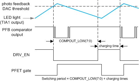
A constant off time feature (see COMPOUT_LOW signal in Figure 18) is included in continuous mode operation. During continuous mode operation, when the desired light level is achieved, the PFET gate drive is turned off by control of the DRV_EN signal and the light level begins to decrease as the inductor current begins to decrease. In a typical hysteretic controller, when a turn on threshold is reached, the PFET is turned on and the light/inductor current increases again. The frequency of switching is dependent on the difference between the turn on and turn off thresholds, loop delay and discrete component values (with the inductor inductance and voltage being most dominant factors).
In the TPS99000-Q1, the control is modified to regulate the operating frequency. A constant off timer is included in the TPS99000-Q1 control loop. When the photo feedback comparator threshold is achieved, a counter is started. The length of the counter is adjustable. While this counter is active, the output of the photo feedback comparator is ignored and the PFET drive (via DRV_EN output from TPS99000-Q1) is disabled. Once the constant off time period counter has expired, the output of the photo feedback comparator is once again used to control the LED current drive. The minimum off-time establishes an upper limit on the hysteretic control loop switching frequency, separate from the natural frequency of the circuit. This feature is useful for assuring the circuit will not operate in the AM radio frequency band, and can also enable the usage of lower inductance value inductors (which can result in system cost savings and power efficiency improvements).
 Figure 18. COMPOUT_LOW Constant Off Time