ZHCSIF5F December 2015 – April 2019 TPS99000-Q1
PRODUCTION DATA.
- 1 特性
- 2 应用
- 3 说明
- 4 修订历史记录
- 5 Pin Configuration and Functions
-
6 Specifications
- 6.1 Absolute Maximum Ratings
- 6.2 ESD Ratings
- 6.3 Recommended Operating Conditions
- 6.4 Thermal Information
- 6.5 Electrical Characteristics - Transimpedance Amplifier Parameters
- 6.6 Electrical Characteristics - Digital to Analog Converters
- 6.7 Electrical Characteristics - Analog to Digital Converter
- 6.8 Electrical Characteristics - FET Gate Drivers
- 6.9 Electrical Characteristics - Photo Comparator
- 6.10 Electrical Characteristics - Voltage Regulators
- 6.11 Electrical Characteristics - Temperature and Voltage Monitors
- 6.12 Electrical Characteristics - Current Consumption
- 6.13 Power-Up Timing Requirements
- 6.14 Power-Down Timing Requirements
- 6.15 Timing Requirements - Sequencer Clock
- 6.16 Timing Requirements - Host / Diagnostic Port SPI Interface
- 6.17 Timing Requirements - ADC Interface
- 6.18 Switching Characteristics
-
7 Detailed Description
- 7.1 Overview
- 7.2 Functional Block Diagram
- 7.3
Feature Description
- 7.3.1
Illumination Control
- 7.3.1.1 Illumination System High Dynamic Range Dimming Overview
- 7.3.1.2 Illumination Control Loop
- 7.3.1.3 Continuous Mode Operation
- 7.3.1.4
Discontinuous Mode Operation
- 7.3.1.4.1 Discontinuous Mode Pulse Width Limit
- 7.3.1.4.2 COMPOUT_LOW Timer in Discontinuous Operation
- 7.3.1.4.3 Dimming Within Discontinuous Operation Range
- 7.3.1.4.4 Multiple Pulse Heights to Increase Bit Depth
- 7.3.1.4.5 TIA Gain Adjustment
- 7.3.1.4.6 Current Limit in Discontinuous Mode
- 7.3.1.4.7 CMODE Big Cap Mode in Discontinuous Operation
- 7.3.2 Over-Brightness Detection
- 7.3.3 Analog to Digital Converter
- 7.3.4 Power Sequencing and Monitoring
- 7.3.5 DMD Mirror Voltage Regulator
- 7.3.6 Low Dropout Regulators
- 7.3.7 System Monitoring Features
- 7.3.8 Communication Ports
- 7.3.1
Illumination Control
- 7.4 Device Functional Modes
- 7.5 Register Maps
- 8 Application and Implementation
- 9 Power Supply Recommendations
- 10Layout
- 11器件和文档支持
- 12机械、封装和可订购信息
封装选项
机械数据 (封装 | 引脚)
- PZP|100
散热焊盘机械数据 (封装 | 引脚)
- PZP|100
订购信息
7.3.1.3.3 Continuous Mode S_EN2 Dissipative Load Shunt Options
The dissipative shunt, enabled by S_EN2 high, can be implemented with a variety of circuit types.
The circuit type selected for the shunt must be able to discharge the inductor used in the LED drive circuit, as well as protect against over voltage conditions on the LED anode voltage.
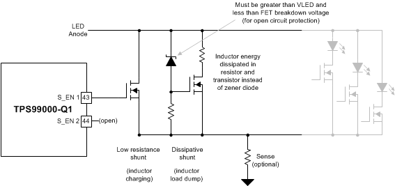
The recommended option is to combine the open circuit protection Zener diode with the S_EN2 dissipative shunt functionality, as shown in Figure 15. This particular option does not connect the S_EN2 pin but still implements the same functionality as the alternate circuits in Figure 14 and Figure 16 which do connect the S_EN2 pin.
 Figure 15. Dissipative Shunt / LED Open Circuit Protection Combination 1
 In this case, a low power Zener diode is used to turn on a FET when the LED anode voltage exceeds the Zener voltage. The S_EN2 enable is not used in this configuration. Rather, the circuit intentionally is placed in an open circuit condition during the S_EN2 blanking time period. Then the protection circuit turns on and drains energy from the inductor (until the S_EN1 shunt is enabled and the LED anode voltage is reduced). The energy in this case is dissipated in a combination of the load resistor and FET. Care must be taken in selection of the Zener diode and resistor divider to ensure the LED anode voltage does not exceed the RGB select FET breakdown voltage. (An option is to delete the load resistor entirely. Then the dissipation will occur only in the FET, and the LED anode voltage will stay closer to the Zener voltage under all conditions). The Zener voltage must be higher than the worst case voltage of input VLED power rail to avoid unintentional triggering of circuit. And Zener voltage must be below the Vds breakdown voltage of the LED selection FETs.
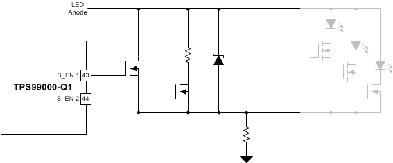
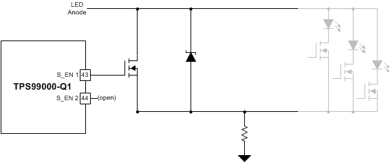
Alternative circuits with the same functionality can be seen below.
 Figure 16. Dissipative Shunt / LED Open Circuit Protection Combination 2
 In this circuit, the inductor current is discharged through the resistive path controlled by S_EN2.
 Figure 17. Dissipative Shunt / LED Open Circuit Protection Combination 3
 In this circuit, the inductor current is discharged through the power Zener diode.