ZHCSQK6 May 2022 TPS92643-Q1
PRODUCTION DATA
- 1 特性
- 2 应用
- 3 说明
- 4 Revision History
- 5 Pin Configuration and Functions
- 6 Specifications
-
7 Detailed Description
- 7.1 Overview
- 7.2 Functional Block Diagram
- 7.3
Feature Description
- 7.3.1 Internal Regulator
- 7.3.2 Buck Converter Switching Operation
- 7.3.3 Bootstrap Supply
- 7.3.4 Switching Frequency and Adaptive On-Time Control
- 7.3.5 Minimum On-Time, Off-Time, and Inductor Ripple
- 7.3.6 LED Current Regulation and Error Amplifier
- 7.3.7 Start-Up Sequence
- 7.3.8 Analog Dimming and Forced Continuous Conduction Mode
- 7.3.9 External PWM Dimming and Input Undervoltage Lockout (UVLO)
- 7.3.10 Analog Pulse Width Modulator Circuit
- 7.3.11 Output Short and Open-Circuit Faults
- 7.3.12 Overcurrent Protection
- 7.3.13 Thermal Shutdown
- 7.3.14 Fault Indicator and Diagnostics Summary
- 7.4 Device Functional Modes
-
8 Application and Implementation
- 8.1
Application Information
- 8.1.1 Duty Cycle Considerations
- 8.1.2 Switching Frequency Selection
- 8.1.3 LED Current Programming
- 8.1.4 Inductor Selection
- 8.1.5 Output Capacitor Selection
- 8.1.6 Input Capacitor Selection
- 8.1.7 Bootstrap Capacitor Selection
- 8.1.8 Bootstrap Resistor Selection
- 8.1.9 Compensation Capacitor Selection
- 8.1.10 Input Dropout and Undervoltage Protection
- 8.1.11 APWM Input and Thermal Protection
- 8.1.12 Protection Diodes
- 8.2
Typical Application
- 8.2.1 Design Requirements
- 8.2.2
Detailed Design Procedure
- 8.2.2.1 Calculating Duty Cycle
- 8.2.2.2 Calculating Minimum On-Time and Off-Time
- 8.2.2.3 Minimum Switching Frequency
- 8.2.2.4 LED Current Set Point
- 8.2.2.5 Inductor Selection
- 8.2.2.6 Output Capacitor Selection
- 8.2.2.7 Bootstrap Capacitor Selection
- 8.2.2.8 Bootstrap Resistor Selection
- 8.2.2.9 Compensation Capacitor Selection
- 8.2.2.10 VIN Dropout Protection and PWM Dimming
- 8.2.3 Application Curves
- 8.1
Application Information
- 9 Power Supply Recommendations
- 10Layout
- 11Device and Documentation Support
- 12Mechanical, Packaging, and Orderable Information
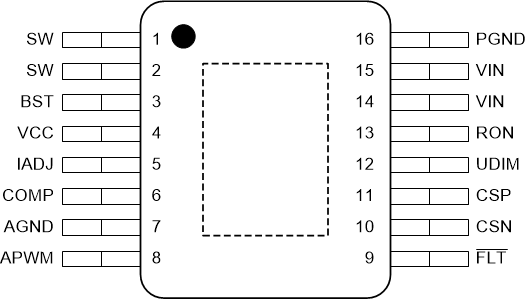
5 Pin Configuration and Functions
 Figure 5-1 PWP Package, 16-Pin HTSSOP
with PowerPAD, Top View
Figure 5-1 PWP Package, 16-Pin HTSSOP
with PowerPAD, Top ViewTable 5-1 Pin Functions
| PIN | I/O | DESCRIPTION | |
|---|---|---|---|
| NO. | NAME | ||
|
7 |
AGND |
— | Analog ground. Return for the internal voltage reference and analog circuit. Connect to circuit ground, GND, to complete return path. |
|
3 |
BST |
I |
Supply input for high-side MOSFET gate drive circuit. Connect a ceramic capacitor between BST and SW pins. An internal diode is connected between VCC and BST pins. |
|
6 |
COMP |
O |
Output of internal transconductance error amplifier. Connect an integral compensation network to ensure stability. |
|
10 |
CSN | I | Negative input (–) of internal rail-to-rail transconductance error amplifier. Connect directly to the negative node of the LED current sense resistor, RCS. |
|
11 |
CSP | I | Positive input (+) of internal rail-to-rail transconductance error amplifier. Connect directly to the positive node of the LED current sense resistor, RCS. |
|
9 |
FLT |
O |
Open-drain fault indicator. Connect to VCC with a resistor to create an active low fault signal output. |
|
5 |
IADJ |
I |
Analog adjust input. Input below 100 mV disables the output. The analog input can be varied between 140 mV to 2.4 V to set current reference from 10 mV to 175 mV. Connect a 0.1-μF capacitor from pin to AGND. |
|
16 |
PGND |
— | Ground returns for low-side MOSFETs |
|
8 |
APWM |
I |
External analog to PWM dimming command. The external analog dimming command between 1 V and 2.45 V is compared to the internal 1.5-kHz triangle waveform to set LED current duty cycle between 0% and 100%. |
|
13 |
RON |
I |
On-time programming pin. Connect a resistor to VIN based on the desired pseudo-fixed switching frequency. |
| 1,2 | SW | I | Switching output of the regulator. Internally connected to both power MOSFETs. Connect to the power inductor. |
|
12 |
UDIM |
I |
Undervoltage lockout and external PWM dimming input. Connect to VIN through a resistor divider to implement input undervoltage protection. Diode couple external PWM signal to enable dimming. Do not float. |
| 4 | VCC | O | VCC bias supply pin. Locally decouple to AGND using a 2.2-μF to 4.7-μF ceramic capacitor located close to the controller. |
| 14,15 | VIN | I | Power input and connection to high-side MOSFET drain node. Connect to the power supply and bypass capacitors CIN. The path from the VIN pin to the high frequency bypass capacitor and PGND must be as short as possible. |
| PowerPAD | — | The AGND and PGND pin must be connected to the exposed PowerPAD for proper operation. This PowerPAD must be connected to PCB ground plane using multiple vias for good thermal performance. | |