ZHCSMJ2 March   2021 TPS92390

PRODUCTION DATA  

  1. 特性
  2. 应用
  3. 说明
  4. Revision History
  5. Pin Configuration and Functions
  6. Specifications
    1. 6.1 Absolute Maximum Ratings
    2. 6.2 ESD Ratings
    3. 6.3 Recommended Operating Conditions
    4. 6.4 Thermal Information
    5. 6.5 Electrical Characteristics
    6. 6.6 Logic Interface Characteristics
    7. 6.7 Timing Requirements for I2C Interface
    8.     14
    9. 6.8 Typical Characteristics
  7. Detailed Description
    1. 7.1 Overview
    2. 7.2 Functional Block Diagram
    3. 7.3 Feature Description
      1. 7.3.1 Control Interface
      2. 7.3.2 Function Setting
      3. 7.3.3 Device Supply (VDD)
      4. 7.3.4 Enable (EN)
      5. 7.3.5 Charge Pump
      6. 7.3.6 Boost Controller
        1. 7.3.6.1 Boost Cycle-by-Cycle Current Limit
        2. 7.3.6.2 Controller Min On/Off Time
        3. 7.3.6.3 Boost Adaptive Voltage Control
          1. 7.3.6.3.1 FB Divider Using Two-Resistor Method
          2. 7.3.6.3.2 FB Divider Using Three-Resistor Method
          3. 7.3.6.3.3 FB Divider Using External Compensation
        4. 7.3.6.4 Boost Sync and Spread Spectrum
        5. 7.3.6.5 Light Load Mode
      7. 7.3.7 LED Current Sinks
        1. 7.3.7.1 LED Output Current Setting
        2. 7.3.7.2 LED Output String Configuration
        3. 7.3.7.3 LED Output PWM Clock Generation
      8. 7.3.8 Brightness Control
        1. 7.3.8.1 Brightness Control Signal Path
        2. 7.3.8.2 Dimming Mode
        3. 7.3.8.3 LED Dimming Frequency
        4. 7.3.8.4 Phase-Shift PWM Mode
        5. 7.3.8.5 Hybrid Mode
        6. 7.3.8.6 Direct PWM Mode
        7. 7.3.8.7 Sloper
        8. 7.3.8.8 PWM Detector Hysteresis
        9. 7.3.8.9 Dither
      9. 7.3.9 Protection and Fault Detections
        1. 7.3.9.1 Supply Faults
          1. 7.3.9.1.1 VIN Undervoltage Faults (VINUVLO)
          2.        51
          3. 7.3.9.1.2 VIN Overvoltage Faults (VINOVP)
          4. 7.3.9.1.3 VDD Undervoltage Faults (VDDUVLO)
          5. 7.3.9.1.4 VIN OCP Faults (VINOCP)
            1. 7.3.9.1.4.1 VIN OCP Current Limit vs. Boost Cycle-by-Cycle Current Limit
          6. 7.3.9.1.5 Charge Pump Faults (CPCAP, CP)
          7. 7.3.9.1.6 CRC Error Faults (CRCERR)
        2. 7.3.9.2 Boost Faults
          1. 7.3.9.2.1 Boost Overvoltage Faults (BSTOVPL, BSTOVPH)
          2. 7.3.9.2.2 Boost Overcurrent Faults (BSTOCP)
          3. 7.3.9.2.3 LEDSET Resistor Missing Faults (LEDSET)
          4. 7.3.9.2.4 MODE Resistor Missing Faults (MODESEL)
          5. 7.3.9.2.5 FSET Resistor Missing Faults (FSET)
          6. 7.3.9.2.6 ISET Resistor Out of Range Faults (ISET)
          7. 7.3.9.2.7 Thermal Shutdown Faults (TSD)
        3. 7.3.9.3 LED Faults
          1. 7.3.9.3.1 Open LED Faults (OPEN_LED)
          2. 7.3.9.3.2 Short LED Faults (SHORT_LED)
          3. 7.3.9.3.3 LED Short to GND Faults (GND_LED)
          4. 7.3.9.3.4 Invalid LED String Faults (INVSTRING)
          5. 7.3.9.3.5 I2C Timeout Faults
        4. 7.3.9.4 Overview of the Fault and Protection Schemes
    4. 7.4 Device Functional Modes
      1. 7.4.1  State Diagram
      2. 7.4.2  Shutdown
      3. 7.4.3  Device Initialization
      4. 7.4.4  Standby Mode
      5. 7.4.5  Power-line FET Soft Start
      6. 7.4.6  Boost Start-Up
      7. 7.4.7  Normal Mode
      8. 7.4.8  Fault Recovery
      9. 7.4.9  Latch Fault
      10. 7.4.10 Start-Up Sequence
    5. 7.5 Programming
      1. 7.5.1 I2C-Compatible Interface
      2. 7.5.2 Programming Examples
        1. 7.5.2.1 General Configuration Registers
        2. 7.5.2.2 Clearing Fault Interrupts
        3. 7.5.2.3 Disabling Fault Interrupts
        4. 7.5.2.4 Diagnostic Registers
    6. 7.6 Register Maps
      1. 7.6.1 FullMap Registers
  8. Application and Implementation
    1. 8.1 Application Information
    2. 8.2 Typical Applications
      1. 8.2.1 Full Feature Application for Display Backlight
        1. 8.2.1.1 Design Requirements
        2. 8.2.1.2 Detailed Design Procedure
          1. 8.2.1.2.1  Inductor Selection
          2. 8.2.1.2.2  Output Capacitor Selection
          3. 8.2.1.2.3  Input Capacitor Selection
          4. 8.2.1.2.4  Charge Pump Output Capacitor
          5. 8.2.1.2.5  Charge Pump Flying Capacitor
          6. 8.2.1.2.6  Output Diode
          7. 8.2.1.2.7  Switching FET
          8. 8.2.1.2.8  Boost Sense Resistor
          9. 8.2.1.2.9  Power-Line FET
          10. 8.2.1.2.10 Input Current Sense Resistor
          11. 8.2.1.2.11 Feedback Resistor Divider
          12. 8.2.1.2.12 Critical Components for Design
        3. 8.2.1.3 Application Curves
      2. 8.2.2 Application With Basic/Minimal Operation
        1. 8.2.2.1 Design Requirements
        2. 8.2.2.2 Detailed Design Procedure
        3. 8.2.2.3 Application Curves
      3. 8.2.3 SEPIC Mode Application
        1. 8.2.3.1 Design Requirements
        2. 8.2.3.2 Detailed Design Procedure
          1. 8.2.3.2.1  Inductor Selection
          2. 8.2.3.2.2  Coupling Capacitor Selection
          3. 8.2.3.2.3  Output Capacitor Selection
          4. 8.2.3.2.4  Input Capacitor Selection
          5. 8.2.3.2.5  Charge Pump Output Capacitor
          6. 8.2.3.2.6  Charge Pump Flying Capacitor
          7. 8.2.3.2.7  Switching FET
          8. 8.2.3.2.8  Output Diode
          9. 8.2.3.2.9  Switching Sense Resistor
          10. 8.2.3.2.10 Power-Line FET
          11. 8.2.3.2.11 Input Current Sense Resistor
          12. 8.2.3.2.12 Feedback Resistor Divider
          13. 8.2.3.2.13 Critical Components for Design
        3. 8.2.3.3 Application Curves
  9. Power Supply Recommendations
  10. 10Layout
    1. 10.1 Layout Guidelines
    2. 10.2 Layout Example
  11. 11Device and Documentation Support
    1. 11.1 Device Support
      1. 11.1.1 第三方产品免责声明
    2. 11.2 接收文档更新通知
    3. 11.3 支持资源
    4. 11.4 Trademarks
    5. 11.5 静电放电警告
    6. 11.6 术语表
  12. 12Mechanical, Packaging, and Orderable Information

封装选项

机械数据 (封装 | 引脚)
散热焊盘机械数据 (封装 | 引脚)
订购信息
FB Divider Using External Compensation

The device has internal compensation network to keep the DC-DC control loop in good stability in most cases. However, an additional external compensation network could also be added on FB-pin to offer more flexibility in loop design or solving some extreme use-cases.

GUID-B1A219BE-F2D6-4049-A51C-317437BE0D52-low.gifFigure 7-7 External Compensation Network

This network will create one additional pole and one additional zero in the loop.

Equation 12. GUID-7877E964-99FC-44A6-8F95-F9042E7459F1-low.gif
Equation 13. GUID-0A1D5FFA-8638-4C20-B6FA-97F0124C2698-low.gif

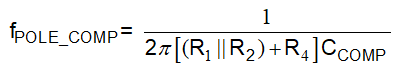
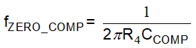
It could be noted that R3 doesn't take part in the compensation. So this external compensation network could be both used in two-divider netwrok and T-divider network with no equation change.

In real application, for example, when DC-DC loop has stability concern, putting the additional pole in 1 kHz and the additional zero in 2 kHz will suppress the loop gain by approximately 6 dB after 2 kHz. This will benefit gain margin and phase margin a lot.