ZHCSOF4A February 2022 – September 2022 TPS7H5005-SEP , TPS7H5006-SEP , TPS7H5007-SEP , TPS7H5008-SEP
PRODUCTION DATA
- 1 特性
- 2 应用
- 3 说明
- 4 Revision History
- 5 Device Comparison Table
- 6 Pin Configuration and Functions
-
7 Specifications
- 7.1 Absolute Maximum Ratings
- 7.2 ESD Ratings
- 7.3 Recommended Operating Conditions
- 7.4 Thermal Information
- 7.5 Electrical Characteristics: All Devices
- 7.6 Electrical Characteristics: TPS7H5005-SEP
- 7.7 Electrical Characteristics: TPS7H5006-SEP
- 7.8 Electrical Characteristics: TPS7H5007-SEP
- 7.9 Electrical Characteristics: TPS7H5008-SEP
- 7.10 Typical Characteristics
-
8 Detailed Description
- 8.1 Overview
- 8.2 Functional Block Diagram
- 8.3
Feature Description
- 8.3.1 VIN and VLDO
- 8.3.2 Start-Up
- 8.3.3 Enable and Undervoltage Lockout (UVLO)
- 8.3.4 Voltage Reference
- 8.3.5 Error Amplifier
- 8.3.6 Output Voltage Programming
- 8.3.7 Soft Start (SS)
- 8.3.8 Switching Frequency and External Synchronization
- 8.3.9 Primary Switching Outputs (OUTA/OUTB)
- 8.3.10 Synchronous Rectifier Outputs (SRA/SRB)
- 8.3.11 Dead Time and Leading Edge Blank Time Programmability (PS, SP, and LEB)
- 8.3.12 Pulse Skipping
- 8.3.13 Duty Cycle Programmability
- 8.3.14 Current Sense and PWM Generation (CS_ILIM)
- 8.3.15 Hiccup Mode Operation (HICC)
- 8.3.16 External Fault Protection (FAULT)
- 8.3.17 Slope Compensation (RSC)
- 8.3.18 Frequency Compensation
- 8.3.19 Thermal Shutdown
- 8.4 Device Functional Modes
-
9 Application and Implementation
- 9.1 Application Information
- 9.2
Typical Application
- 9.2.1 Design Requirements
- 9.2.2
Detailed Design Procedure
- 9.2.2.1 Switching Frequency
- 9.2.2.2 Output Voltage Programming Resistors
- 9.2.2.3 Dead Time
- 9.2.2.4 Leading Edge Blank Time
- 9.2.2.5 Soft-Start Capacitor
- 9.2.2.6 Transformer
- 9.2.2.7 Main Switching FETs
- 9.2.2.8 Synchronous Rectificier FETs
- 9.2.2.9 RCD Clamp
- 9.2.2.10 Output Inductor
- 9.2.2.11 Output Capacitance and Filter
- 9.2.2.12 Sense Resistor
- 9.2.2.13 Hiccup Capacitor
- 9.2.2.14 Frequency Compensation Components
- 9.2.2.15 Slope Compensation Resistor
- 10Power Supply Recommendations
- 11Layout
- 12Device and Documentation Support
- 13Mechanical, Packaging, and Orderable Information
9.2.2.11 Output Capacitance and Filter
Generally, there are two different calculations that can be used to determine the output capacitance required for the converter. The first calculates the amount of capacitance required to meet the maximum allowable voltage deviation at the output in response to a worst-case load transient as shown in Equation 62. The second, shown in Equation 64, determines the amount of output capacitance that is needed to meet the output voltage ripple requirements of the design. Once the two different calculations are performed, the maximum of these should be chosen as the output capacitance for the design. The calculations are shown for target voltage ripple of 2% of the output voltage and maximum allowable voltage deviation of 2.5% of the output voltage.
Based on the calculations, at least 1.3 mF of output capacitance is required. When selecting capacitors, consider any derating of capacitance that is needed to account for aging, temperature, and DC bias.
For space-grade converter designs, there is another consideration when selecting the output capacitance. This is the impact of radiation induced single event transients (SETs). Single energetic particle strikes can lead to momentary variation in the PWM operation of the controller, which in turn can lead to output voltage transients in the converter. Thus, even though the value above provides a minimum value to account for voltage ripple and/or load transients, additional capacitance is likely needed to for adequate SET mitigation. For the design example, approximately 2.3 mF of total output capacitance was used.
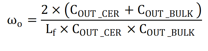
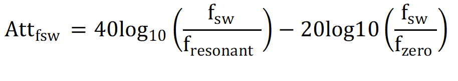
An additional output filter can be used to further reduce the noise of the output stage if deemed necessary. This output filter consists of an additional inductor and a small amount of ceramic capacitance. This ceramic capacitance is placed immediately downstream of the main output inductor that was determined in Section 9.2.2.10. The filter inductance is then located between the added ceramic capacitance and the bulk output capacitance that was determined to be required for the design. This approach can drastically reduce the output voltage ripple without significantly increasing the size and/or number of components required. The key for the secondary filter design is to choose the resonant frequency such that it is higher than the targeted crossover frequency yet well below the switching frequency and ESR zero of the bulk output capacitance. Equation 66, Equation 67, and Equation 68 can be used to determine the ESR zero as well as the resonant frequency and attenuation of the additional output filter.
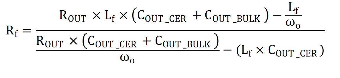
In the event that there is peaking at high frequencies due to the output filter, a resistor can be used to dampen this peaking effect. Equation 69 and Equation 70 can be used to determine the frequency of the peaking and the value of the resistor needed to provide adequate damping.