ZHCSL64D april 2019 – may 2023 TPS7H4001-SP
PRODMIX
- 1
- 1 特性
- 2 应用
- 3 说明
- 4 Revision History
- 5 Device Options Table
- 6 Pin Configuration and Functions
-
7 Specifications
- 7.1 Absolute Maximum Ratings
- 7.2 ESD Ratings
- 7.3 Recommended Operating Conditions
- 7.4 Thermal Information
- 7.5 Electrical Characteristics - All Devices
- 7.6 Electrical Characteristics: CDFP and KGD Options
- 7.7 Electrical Characteristics: HTSSOP (SHP) Option
- 7.8 Electrical Characteristics: HTSSOP (QMLP) Option
- 7.9 Quality Conformance Inspection
- 7.10 Typical Characteristics
-
8 Detailed Description
- 8.1 Overview
- 8.2 Functional Block Diagram
- 8.3
Feature Description
- 8.3.1 VIN and Power VIN Pins (VIN and PVIN)
- 8.3.2 Voltage Reference
- 8.3.3 Adjusting the Output Voltage
- 8.3.4 Safe Start-Up Into Prebiased Outputs
- 8.3.5 Error Amplifier
- 8.3.6 Enable and Adjust UVLO
- 8.3.7 Adjustable Switching Frequency and Synchronization (SYNC)
- 8.3.8 Soft-Start (SS/TR)
- 8.3.9 Power Good (PWRGD)
- 8.3.10 Sequencing
- 8.3.11 Output Overvoltage Protection (OVP)
- 8.3.12 Overcurrent Protection
- 8.3.13 Thermal Shutdown
- 8.3.14 Turn-On Behavior
- 8.3.15 Slope Compensation
- 8.3.16 Small Signal Model for Frequency Compensation
- 8.4 Device Functional Modes
-
9 Application and Implementation
- 9.1 Application Information
- 9.2
Typical Application
- 9.2.1 Design Requirements
- 9.2.2
Detailed Design Procedure
- 9.2.2.1 Operating Frequency
- 9.2.2.2 Output Inductor Selection
- 9.2.2.3 Output Capacitor Selection
- 9.2.2.4 Input Capacitor Selection
- 9.2.2.5 Soft-Start Capacitor Selection
- 9.2.2.6 Undervoltage Lockout (UVLO) Set Point
- 9.2.2.7 Output Voltage Feedback Resistor Selection
- 9.2.2.8 Compensation Component Selection
- 9.2.3 Parallel Operation
- 9.2.4 Application Curve
- 9.3 Power Supply Recommendations
- 9.4 Layout
- 10Device and Documentation Support
- 11Mechanical, Packaging, and Orderable Information
封装选项
请参考 PDF 数据表获取器件具体的封装图。
机械数据 (封装 | 引脚)
- DDW|44
- KGD|0
- HKY|34
散热焊盘机械数据 (封装 | 引脚)
- DDW|44
订购信息
8.3.6 Enable and Adjust UVLO
The EN pin provides electrical on and off control of the device. When the EN pin voltage exceeds the threshold voltage, the device enables operation. If the EN pin voltage is pulled below the threshold voltage, the regulator stops switching and enters low Iq state. The EN pin has an internal pullup current source, allowing the user to float the EN pin for enabling the device. If an application requires controlling the EN pin, use open-drain or open-collector output logic to interface with the pin.
The device implements internal UVLO circuitry on the VIN pin. The device is disabled when the VIN pin voltage falls below the internal VIN UVLO threshold. The internal VIN UVLO threshold has a hysteresis of 150-mV typical.
If an application requires either a higher UVLO threshold on the VIN pin or a secondary UVLO on the PVIN in split-rail applications, then the EN pin can be configured as shown in Figure 8-1, Figure 8-2, and Figure 8-3. A ceramic capacitor in parallel with the bottom resistor R2 is recommended to reduce noise on the EN pin as used in the TPS7H4001-SP Evaluation Module. See the TPS7H4001EVM-CVAL Evaluation Module (EVM) User's Guide (SLVUBO5) for more information.
The EN pin has a small pullup current, Ip, which sets the default state of the pin to enable when no external components are connected. The pullup current is also used to control the voltage hysteresis for the UVLO function because it increases by Ih after the EN pin crosses the enable threshold. Calculate the UVLO thresholds with Equation 2 and Equation 3.
 Figure 8-1 Adjustable VIN UVLO
 Figure 8-2 Adjustable PVIN UVLO
 Figure 8-3 Adjustable VIN and PVIN UVLO
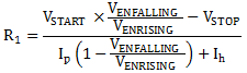
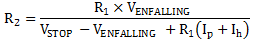
where
- Ih = 3 μA
- Ip = 6.1 μA
- VENRISING = 1.14 V
- VENFALLING = 1.11 V