SBVS064N December 2005 – November 2016 TPS74201
PRODUCTION DATA.
- 1 Features
- 2 Applications
- 3 Description
- 4 Revision History
- 5 Pin Configuration and Functions
- 6 Specifications
- 7 Detailed Description
- 8 Application and Implementation
- 9 Power Supply Recommendations
- 10Layout
- 11Device and Documentation Support
- 12Mechanical, Packaging, and Orderable Information
封装选项
机械数据 (封装 | 引脚)
散热焊盘机械数据 (封装 | 引脚)
订购信息
7 Detailed Description
7.1 Overview
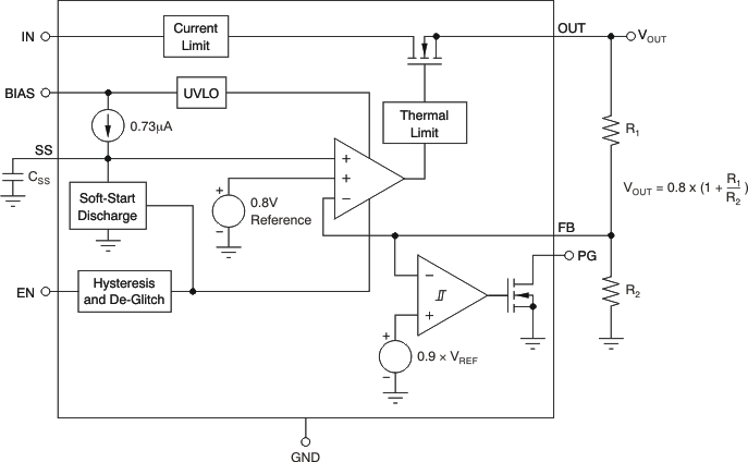
The TPS742 belongs to a family of generation ultra-low dropout regulators that feature soft-start and tracking capabilities. These regulators use a low current bias input to power all internal control circuitry, allowing the NMOS pass transistor to regulate very low input and output voltages.
The use of an NMOS-pass FET offers several critical advantages for many applications. Unlike a PMOS topology device, the output capacitor has little effect on loop stability. This architecture allows the TPS742 devices to be stable with any or even no output capacitor. Transient response is also superior to PMOS topologies, particularly for low VIN applications.
The TPS742 devices feature a programmable voltage-controlled soft-start circuit that provides a smooth, monotonic start-up and limits start-up inrush currents that may be caused by large capacitive loads. A power-good (PG) output is available to allow supply monitoring and sequencing of other supplies. An enable (EN) pin with hysteresis and deglitch allows slow-ramping signals to be used for sequencing the device. The low VIN and VOUT capability allows for inexpensive, easy-to-design, and efficient linear regulation between the multiple supply voltages often present in processor intensive systems.
7.2 Functional Block Diagram

7.3 Feature Description
7.3.1 Enable and Shutdown
The enable (EN) pin is active high and is compatible with standard digital signaling levels. VEN less than 0.4 V turns the regulator off and VEN greater than 1.1 V turns the regulator on. Unlike many regulators, the enable circuitry has hysteresis and deglitching for use with relatively slow-ramping analog signals. This configuration allows the TPS742 devices to be enabled by connecting the output of another supply to the EN pin. The enable circuitry typically has 50 mV of hysteresis and a deglitch circuit to help avoid ON and OFF cycling because of small glitches in the VEN signal.
The enable threshold is typically 0.8 V and varies with temperature and process variations. Temperature variation is approximately –1 mV/°C; therefore, process variation accounts for most of the variation in the enable threshold. If precise turnon timing is required, then use a fast rise-time signal to enable the TPS742 devices.
If not used, EN can be connected to either IN or BIAS. If EN is connected to IN, then connect EN as closely as possible to the largest capacitance on the input to prevent voltage droops on that line from triggering the enable circuit.
7.3.2 Power-Good (VQFN Packages Only)
The power-good (PG) pin is an open-drain output and can be connected to any 5.5 V or lower rail through an external pullup resistor. This pin requires at least 1.1 V on VBIAS to have a valid output. The PG output is high-impedance when VOUT is greater than VIT + VHYS. If VOUT drops below VIT or if VBIAS drops less than 1.9 V, the open-drain output turns on and pulls the PG output low. The PG pin also asserts when the device is disabled. The recommended operating condition of PG pin sink current is up to 1 mA, so the pullup resistor for PG must be in the range of 10 kΩ to 1 MΩ. PG is only provided on the VQFN packages. If output voltage monitoring is not needed, then the PG pin can be left floating.
7.3.3 Internal Current Limit
The TPS742 family features a factory-trimmed, accurate current limit that is flat over temperature and supply voltage. The current limit allows the device to supply surges of up to 1.8 A and maintain regulation. The current limit responds in about 10 μs to reduce the current during a short circuit fault. Recovery from a short circuit condition is well-controlled and results in very little output overshoot when the load is removed. See Figure 23 in the Typical Characteristics section for a graph of IOUT versus VOUT performance.
The internal current limit protection circuitry of the TPS742 family of devices is designed to protect against overload conditions. The circuitry is not intended to allow operation above the rated current of the device. Continuously running the TPS742 devices above the rated current degrades device reliability.
7.4 Device Functional Modes
7.4.1 Normal Operation
The device regulates to the nominal output voltage under the following conditions:
- The input voltage and bias voltage are both at least at the respective minimum specifications.
- The enable voltage has previously exceeded the enable rising threshold voltage and has not decreased below the enable falling threshold.
- The output current is less than the current limit.
- The device junction temperature is less than the maximum specified junction temperature.
- The device is not operating in dropout.
7.4.2 Dropout Operation
If the input voltage is lower than the nominal output voltage plus the specified dropout voltage, but all other conditions are met for normal operation, the device operates in dropout mode. In this condition, the output voltage is the same as the input voltage minus the dropout voltage. The transient performance of the device is significantly degraded because the pass device is in a triode state and no longer controls the current through the LDO. Line or load transients in dropout can result in large output voltage deviations.
7.4.3 Disabled
The device is disabled under the following conditions:
- The input or bias voltages are below the respective minimum specifications.
- The enable voltage is less than the enable falling threshold voltage or has not yet exceeded the enable rising threshold.
- The device junction temperature is greater than the thermal shutdown temperature.
Table 1 shows the conditions that lead to the different modes of operation.