SBVS038U September 2003 – January 2015 TPS736
PRODUCTION DATA.
- 1 Features
- 2 Applications
- 3 Description
- 4 Revision History
- 5 Pin Configuration and Functions
- 6 Specifications
- 7 Detailed Description
- 8 Application and Implementation
- 9 Power Supply Recommendations
- 10Layout
- 11Device and Documentation Support
- 12Mechanical, Packaging, and Orderable Information
封装选项
机械数据 (封装 | 引脚)
散热焊盘机械数据 (封装 | 引脚)
- DRB|8
订购信息
7 Detailed Description
7.1 Overview
The TPS736xx family of low-dropout linear regulators operates down to an input voltage of 1.7 V and supports output voltages down to 1.2 V while sourcing up to 500 mA of load current. This linear regulator utilizes an NMOS pass element with an integrated 4-MHz charge pump to provide a dropout voltage of less than 200 mV at full load current. This unique architecture also permits stable regulation over a wide range of output capacitors. In fact, the TPS736xx family of devices does not require any output capacitor for stability. The increased insensitivity to the output capacitor value and type makes this family of linear regulators an ideal choice when powering a load where the effective capacitance is unknown.
The TPS736xx family of devices also features a noise reduction (NR) pin that allows for additional reduction of the output noise. With a noise reduction capacitor of 0.01 µF connected from the NR pin to GND, the TPS73615 output noise can be as low as 12.75 µVRMS. The low noise output featured by the TPS736xx family makes it well-suited for powering VCOs or any other noise sensitive load.
7.2 Functional Block Diagram
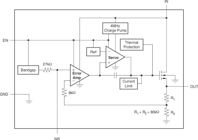 Figure 29. Fixed-Voltage Version
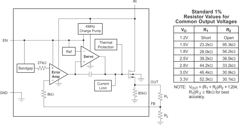 Figure 30. Adjustable-Voltage Version
7.3 Feature Description
7.3.1 Output Noise
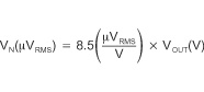
A precision band-gap reference is used to generate the internal reference voltage, VREF. This reference is the dominant noise source within the TPS736xx and it generates approximately 32 μVRMS (10 Hz to 100 kHz) at the reference output (NR). The regulator control loop gains up the reference noise with the same gain as the reference voltage, so that the noise voltage of the regulator is approximately given by:
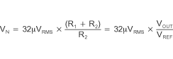
Since the value of VREF is 1.2 V, this relationship reduces to:
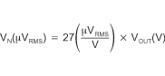
for the case of no CNR.
An internal 27-kΩ resistor in series with the noise reduction pin (NR) forms a low-pass filter for the voltage reference when an external noise reduction capacitor, CNR, is connected from NR to ground. For CNR = 10 nF, the total noise in the 10-Hz to 100-kHz bandwidth is reduced by a factor of ~3.2, giving the approximate relationship:
for CNR = 10 nF.
This noise reduction effect is shown as RMS Noise Voltage vs CNR in the Typical Characteristics section.
The TPS73601 adjustable version does not have the NR pin available. However, connecting a feedback capacitor, CFB, from the output to the feedback pin (FB) reduces output noise and improves load transient performance.
The TPS736xx uses an internal charge pump to develop an internal supply voltage sufficient to drive the gate of the NMOS pass element above VOUT. The charge pump generates ~250 μV of switching noise at ~4 MHz; however, charge-pump noise contribution is negligible at the output of the regulator for most values of IOUT and COUT.
7.3.2 Internal Current Limit
The TPS736xx internal current limit helps protect the regulator during fault conditions. Foldback current limit helps to protect the regulator from damage during output short-circuit conditions by reducing current limit when VOUT drops below 0.5 V. See Figure 10 in the Typical Characteristics section.
Note from Figure 10 that approximately –0.2 V of VOUT results in a current limit of 0 mA. Therefore, if OUT is forced below –0.2 V before EN goes high, the device may not start up. In applications that work with both a positive and negative voltage supply, the TPS736xx should be enabled first.
7.3.3 Enable Pin and Shutdown
The enable pin (EN) is active high and is compatible with standard TTL-CMOS levels. VEN below 0.5 V (max) turns the regulator off and drops the GND pin current to approximately 10 nA. When EN is used to shutdown the regulator, all charge is removed from the pass transistor gate, and the output ramps back up to a regulated VOUT (see Figure 19).
When shutdown capability is not required, EN can be connected to VIN. However, the pass gate may not be discharged using this configuration, and the pass transistor may be left on (enhanced) for a significant time after VIN has been removed. This scenario can result in reverse current flow (if the IN pin is low impedance) and faster ramp times upon power-up. In addition, for VIN ramp times slower than a few milliseconds, the output may overshoot upon power-up.
Note that current limit foldback can prevent device start-up under some conditions. See the Internal Current Limit section for more information.
7.3.4 Reverse Current
The NMOS pass element of the TPS736xx provides inherent protection against current flow from the output of the regulator to the input when the gate of the pass device is pulled low. To ensure that all charge is removed from the gate of the pass element, the EN pin must be driven low before the input voltage is removed. If this is not done, the pass element may be left on due to stored charge on the gate.
After the EN pin is driven low, no bias voltage is needed on any pin for reverse current blocking. Note that reverse current is specified as the current flowing out of the IN pin due to voltage applied on the OUT pin. There is additional current flowing into the OUT pin due to the 80-kΩ internal resistor divider to ground (see Figure 29and Figure 30).
For the TPS73601, reverse current may flow when VFB is more than 1.0 V above VIN.
7.4 Device Functional Modes
7.4.1 Normal Operation with 1.7 V ≤ VIN ≤ 5.5 V and VEN ≥ 1.7 V
The TPS736xx family requires an input voltage of at least 1.7 V to function properly and attempt to maintain regulation. Please note that if the device output voltage is greater than 1.5 V when the input voltage is at 1.7 V, the device is operating in dropout and regulation cannot be maintained. Due the NMOS architecture used in the TPS736xx devices, the dropout voltage is not a strong function of the input voltage.
When operating the device near 5.5 V, take care to suppress any transient spikes that may exceed the 6.0-V absolute maximum voltage rating. The device should never operate at a dc voltage greater than 5.5 V.