ZHCSNK8 March 2021 TPS62810M , TPS62811M , TPS62812M , TPS62813M
PRODUCTION DATA
- 1 特性
- 2 应用
- 3 说明
- 4 Revision History
- 5 Device Comparison Table
- 6 Pin Configuration and Functions
- 7 Specifications
- 8 Parameter Measurement Information
- 9 Detailed Description
- 10Application and Implementation
- 11Power Supply Recommendations
- 12Layout
- 13Device and Documentation Support
- 14Mechanical, Packaging, and Orderable Information
6 Pin Configuration and Functions
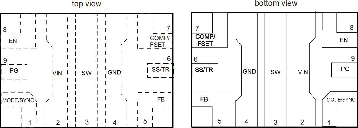
 Figure 6-1 9-Pin (VQFN) RWY
Package
Figure 6-1 9-Pin (VQFN) RWY
PackageTable 6-1 Pin Functions
| PIN | I/O | DESCRIPTION | |
|---|---|---|---|
| NAME | NO. | ||
| EN | 8 | I | This is the enable pin of the device. Connect to logic low to disable the device. Pull high to enable the device. Do not leave this pin unconnected. |
| FB | 5 | I | Voltage feedback input. Connect the resistive output voltage divider to this pin. For the fixed voltage versions, connect the FB pin directly to the output voltage. |
| GND | 4 | Ground pin | |
| MODE/SYNC | 1 | I | The device runs in PFM/PWM mode when this pin is pulled low. If the pin is pulled high, the device runs in forced PWM mode. Do not leave this pin unconnected. The mode pin can also be used to synchronize the device to an external frequency. See Section 7 for the detailed specification of the digital signal applied to this pin for external synchronization. |
| COMP/FSET | 7 | I | Device compensation and frequency set input. A resistor from this pin to GND defines the compensation of the control loop as well as the switching frequency if not externally synchronized. If the pin is tied to GND or VIN, the switching frequency is set to 2.25 MHz. Do not leave this pin unconnected. |
| PG | 9 | O | Open-drain power-good output. Low impedance when not "power good", high impedance when "power good". This pin can be left open or be tied to GND when not used. |
| SS/TR | 6 | I | Soft Start / Tracking pin. A capacitor connected from this pin to GND defines the rise time for the internal reference voltage. The pin can also be used as an input for tracking and sequencing; see Section 9.4.7. |
| SW | 3 | Switch pin of the converter. This pin is connected to the internal power MOSFETs. | |
| VIN | 2 | Power supply input. Connect the input capacitor as close as possible between the VIN pin and GND. | |