ZHCSHZ2E December 2014 – March 2022 TPS62406-Q1 , TPS62407-Q1 , TPS62422-Q1 , TPS62423-Q1 , TPS62424-Q1
PRODUCTION DATA
- 1 特性
- 2 应用
- 3 说明
- 4 Revision History
- 5 Device Comparison Table
- 6 Pin Configuration and Functions
- 7 Specifications
- 8 Detailed Description
- 9 Application and Implementation
- 10Power Supply Recommendations
- 11Layout
- 12Device and Documentation Support
- 13Mechanical, Packaging, and Orderable Information
8.5.1.3 Mode Selection
Use of the MODE/DATA pin for two functions, interface and mode selection, necessitates a determination of when to decode the bit stream or to change the operation mode.
The device enters forced PWM mode operation immediately whenever the MODE/DATA pin turns to high level. The device also stays in forced PWM mode during the entire protocol reception time.
With a falling edge on the MODE/DATA pin, the device starts bit decoding. If the MODE/DATA pin stays low for at least ttimeout, the device gets an internal time-out and enables power-save-mode operation.
The device ignores a protocol sent within this time because the first interpretation of a falling edge for the mode change is at the start of the first bit. In this case, TI recommends sending the protocol first, and then changing to power-save mode at the end of the protocol.
 Figure 8-3 EasyScale Protocol Overview
| BYTE | BIT NUMBER | NAME | TRANSMISSION DIRECTION | DESCRIPTION |
|---|---|---|---|---|
| Device address byte | 7 | DA7 | IN | 0 MSB device address |
| 6 | DA6 | IN | 1 | |
| 5 | DA5 | IN | 0 | |
| 4 | DA4 | IN | 0 | |
| 4E hex | 3 | DA3 | IN | 1 |
| 2 | DA2 | IN | 1 | |
| 1 | DA1 | IN | 1 | |
| 0 | DA0 | IN | 0 LSB device address | |
| Data byte | 7 (MSB) | RFA | IN | Request for acknowledge; if high, the device applies an acknowledge condition. |
| 6 | A1 | Address bit 1 | ||
| 5 | A0 | Address bit 0 | ||
| 4 | D4 | Data bit 4 | ||
| 3 | D3 | Data bit 3 | ||
| 2 | D2 | Data bit 2 | ||
| 1 | D1 | Data bit 1 | ||
| 0 (LSB) | D0 | Data bit 0 | ||
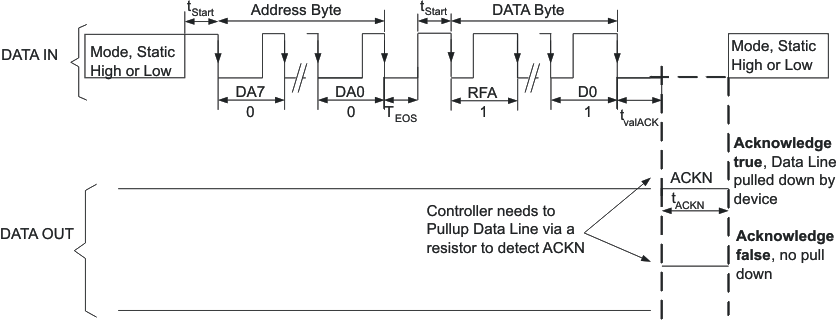
| ACK | OUT | Acknowledge condition active 0, the device applies this condition only in the case of a set RFA bit. Open-drain output, the host must pull the line high with a pullup resistor. | ||
| One can only use this feature if the master has an open-drain output stage. In case of a push-pull output stage, do not request an acknowledge condition. |
 Figure 8-4 EasyScale Protocol Without Acknowledge
 Figure 8-5 EasyScale Protocol Including Acknowledge
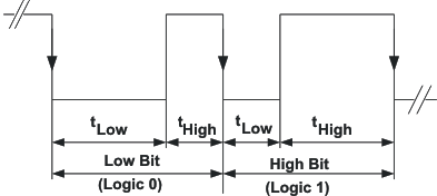
 Figure 8-6 EasyScale – Bit Coding
 Figure 8-7 MODE/DATA PIN: Mode Selection
 Figure 8-8 MODE/DATA Pin: Power-Save-Mode and Interface Communication
With Pin DEF_1 as Digital Input
| TPS624xx-Q1 OUTPUT VOLTAGE [V] REGISTER REG_DEF_1_LOW | TPS624xx-Q1 VOLTAGE [V] REGISTER REG_DEF_1_HIGH | D4 | D3 | D2 | D1 | D0 | |
|---|---|---|---|---|---|---|---|
| 0 | 0.8 | 0.9 | 0 | 0 | 0 | 0 | 0 |
| 1 | 0.825 | 0.925 | 0 | 0 | 0 | 0 | 1 |
| 2 | 0.85 | 0.95 | 0 | 0 | 0 | 1 | 0 |
| 3 | 0.875 | 0.975 | 0 | 0 | 0 | 1 | 1 |
| 4 | 0.9 | 1.0 | 0 | 0 | 1 | 0 | 0 |
| 5 | 0.925 | 1.025 | 0 | 0 | 1 | 0 | 1 |
| 6 | 0.95 | 1.050 | 0 | 0 | 1 | 1 | 0 |
| 7 | 0.975 | 1.075 | 0 | 0 | 1 | 1 | 1 |
| 8 | 1.0 | 1.1 | 0 | 1 | 0 | 0 | 0 |
| 9 | 1.025 | 1.125 | 0 | 1 | 0 | 0 | 1 |
| 10 | 1.050 | 1.150 | 0 | 1 | 0 | 1 | 0 |
| 11 | 1.075 | 1.175 | 0 | 1 | 0 | 1 | 1 |
| 12 | 1.1 | 1.2 | 0 | 1 | 1 | 0 | 0 |
| 13 | 1.125 | 1.225 | 0 | 1 | 1 | 0 | 1 |
| 14 | 1.150 | 1.25 | 0 | 1 | 1 | 1 | 0 |
| 15 | 1.175 | 1.275 | 0 | 1 | 1 | 1 | 1 |
| 16 | 1.2 | 1.3 | 1 | 0 | 0 | 0 | 0 |
| 17 | 1.225 | 1.325 | 1 | 0 | 0 | 0 | 1 |
| 18 | 1.25 | 1.350 | 1 | 0 | 0 | 1 | 0 |
| 19 | 1.275 | 1.375 | 1 | 0 | 0 | 1 | 1 |
| 20 | 1.3 | 1.4 | 1 | 0 | 1 | 0 | 0 |
| 21 | 1.325 | 1.425 | 1 | 0 | 1 | 0 | 1 |
| 22 | 1.350 | 1.450 | 1 | 0 | 1 | 1 | 0 |
| 23 | 1.375 | 1.475 | 1 | 0 | 1 | 1 | 1 |
| 24 | 1.4 | 1.5 | 1 | 1 | 0 | 0 | 0 |
| 25 | 1.425 | 1.525 | 1 | 1 | 0 | 0 | 1 |
| 26 | 1.450 | 1.55 | 1 | 1 | 0 | 1 | 0 |
| 27 | 1.475 | 1.575 | 1 | 1 | 0 | 1 | 1 |
| 28 | 1.5 | 1.6 | 1 | 1 | 1 | 0 | 0 |
| 29 | 1.525 | 1.7 | 1 | 1 | 1 | 0 | 1 |
| 30 | 1.55 | 1.8 | 1 | 1 | 1 | 1 | 0 |
| 31 | 1.575 | 1.9 | 1 | 1 | 1 | 1 | 1 |
(ADJ2 Connected to VOUT2)
| OUTPUT VOLTAGE [V] FOR REGISTER REG_DEF_2 | D4 | D3 | D2 | D1 | D0 | |
|---|---|---|---|---|---|---|
| 0 | 0.6 | 0 | 0 | 0 | 0 | 0 |
| 1 | 0.85 | 0 | 0 | 0 | 0 | 1 |
| 2 | 0.9 | 0 | 0 | 0 | 1 | 0 |
| 3 | 0.95 | 0 | 0 | 0 | 1 | 1 |
| 4 | 1 | 0 | 0 | 1 | 0 | 0 |
| 5 | 1.05 | 0 | 0 | 1 | 0 | 1 |
| 6 | 1.1 | 0 | 0 | 1 | 1 | 0 |
| 7 | 1.15 | 0 | 0 | 1 | 1 | 1 |
| 8 | 1.2 | 0 | 1 | 0 | 0 | 0 |
| 9 | 1.25 | 0 | 1 | 0 | 0 | 1 |
| 10 | 1.3 | 0 | 1 | 0 | 1 | 0 |
| 11 | 1.35 | 0 | 1 | 0 | 1 | 1 |
| 12 | 1.4 | 0 | 1 | 1 | 0 | 0 |
| 13 | 1.45 | 0 | 1 | 1 | 0 | 1 |
| 14 | 1.5 | 0 | 1 | 1 | 1 | 0 |
| 15 | 1.55 | 0 | 1 | 1 | 1 | 1 |
| 16 | 1.6 | 1 | 0 | 0 | 0 | 0 |
| 17 | 1.7 | 1 | 0 | 0 | 0 | 1 |
| 18 | 1.8 | 1 | 0 | 0 | 1 | 0 |
| 19 | 1.85 | 1 | 0 | 0 | 1 | 1 |
| 20 | 2 | 1 | 0 | 1 | 0 | 0 |
| 21 | 2.1 | 1 | 0 | 1 | 0 | 1 |
| 22 | 2.2 | 1 | 0 | 1 | 1 | 0 |
| 23 | 2.3 | 1 | 0 | 1 | 1 | 1 |
| 24 | 2.4 | 1 | 1 | 0 | 0 | 0 |
| 25 | 2.5 | 1 | 1 | 0 | 0 | 1 |
| 26 | 2.6 | 1 | 1 | 0 | 1 | 0 |
| 27 | 2.7 | 1 | 1 | 0 | 1 | 1 |
| 28 | 2.8 | 1 | 1 | 1 | 0 | 0 |
| 29 | 2.85 | 1 | 1 | 1 | 0 | 1 |
| 30 | 3 | 1 | 1 | 1 | 1 | 0 |
| 31 | 3.3 | 1 | 1 | 1 | 1 | 1 |