ZHCSHZ2E December   2014  – March 2022 TPS62406-Q1 , TPS62407-Q1 , TPS62422-Q1 , TPS62423-Q1 , TPS62424-Q1

PRODUCTION DATA  

  1. 特性
  2. 应用
  3. 说明
  4. Revision History
  5. Device Comparison Table
  6. Pin Configuration and Functions
  7. Specifications
    1. 7.1 Absolute Maximum Ratings
    2. 7.2 ESD Ratings
    3. 7.3 Recommended Operating Conditions
    4. 7.4 Thermal Information
    5. 7.5 Electrical Characteristics
    6. 7.6 Timing Requirements
    7. 7.7 Switching Characteristics
    8. 7.8 Typical Characteristics
  8. Detailed Description
    1. 8.1 Overview
      1. 8.1.1 Converter 1
      2. 8.1.2 Converter 2
    2. 8.2 Functional Block Diagram
    3. 8.3 Feature Description
      1. 8.3.1 Enable
      2. 8.3.2 DEF_1 Pin Function
      3. 8.3.3 180° Out-of-Phase Operation
      4. 8.3.4 Short-Circuit Protection
      5. 8.3.5 Thermal Shutdown
      6. 8.3.6 EasyScale Interface: One-Pin Serial Interface for Dynamic Output-Voltage Adjustment
        1. 8.3.6.1 General
        2. 8.3.6.2 Protocol
    4. 8.4 Device Functional Modes
      1. 8.4.1 Power-Save Mode
        1. 8.4.1.1 Dynamic Voltage Positioning
        2. 8.4.1.2 Soft Start
        3. 8.4.1.3 100% Duty-Cycle Low-Dropout Operation
        4. 8.4.1.4 Undervoltage Lockout
      2. 8.4.2 Mode Selection
    5. 8.5 Programming
      1. 8.5.1 Addressable Registers
        1. 8.5.1.1 Bit Decoding
        2. 8.5.1.2 Acknowledge
        3. 8.5.1.3 Mode Selection
  9. Application and Implementation
    1. 9.1 Application Information
      1. 9.1.1 Application Information
    2. 9.2 Typical Application
      1. 9.2.1 Design Requirements
      2. 9.2.2 Detailed Design Procedure
        1. 9.2.2.1 Output Voltage Setting
          1. 9.2.2.1.1 Converter 1 Fixed Default Output-Voltage Setting
          2. 9.2.2.1.2 Converter 2 Fixed Default Output-Voltage Setting
        2. 9.2.2.2 Output Filter Design (Inductor and Output Capacitor)
          1. 9.2.2.2.1 Inductor Selection
          2. 9.2.2.2.2 Output-Capacitor Selection
          3. 9.2.2.2.3 Input Capacitor Selection
      3. 9.2.3 Application Curves
    3. 9.3 System Examples
  10. 10Power Supply Recommendations
  11. 11Layout
    1. 11.1 Layout Guidelines
    2. 11.2 Layout Example
  12. 12Device and Documentation Support
    1. 12.1 支持资源
    2. 12.2 接收文档更新通知
    3. 12.3 Trademarks
    4. 12.4 Electrostatic Discharge Caution
    5. 12.5 术语表
  13. 13Mechanical, Packaging, and Orderable Information

封装选项

机械数据 (封装 | 引脚)
散热焊盘机械数据 (封装 | 引脚)
订购信息
Output-Capacitor Selection

The advanced fast-response voltage-mode control scheme of the converters allows the use of tiny ceramic capacitors with a typical value of 10 μF to 22 μF, without having large output-voltage under- and overshoots during heavy load transients. Ceramic capacitors with low ESR values result in lowest output-voltage ripple, and TI therefore recommends them. The output capacitor requires either X7R or X5R dielectric. TI does not recommend Y5V and Z5U dielectric capacitors because of their wide variation in capacitance.

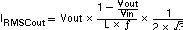
If using ceramic output capacitors, the capacitor rms ripple-current rating always meets the application requirements. The rms ripple current calculation is:

Equation 6. GUID-2EC6BD14-85DE-48AE-A338-75EDA1E105C5-low.gif

At nominal load current, the inductive converters operate in PWM mode and the overall output voltage ripple is the sum of the voltage spike caused by the output capacitor ESR, plus the voltage ripple caused by charging and discharging the output capacitor:
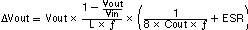
Equation 7. GUID-F6EBA3D7-A731-41FF-B833-696086FBCC5C-low.gif

where

  • The highest output-voltage ripple occurs at the highest input voltage, VIN.

At light load currents, the converters operate in power-save mode and the output-voltage ripple depends on the output-capacitor value. The internal comparator delay and the external capacitor set the output-voltage ripple. Higher output capacitors like 22 μF values minimize the voltage ripple in PFM mode and tighten dc output accuracy in PFM mode.