SLVS681F June 2006 – August 2014 TPS62400 , TPS62401 , TPS62402 , TPS62403 , TPS62404
PRODUCTION DATA.
- 1 Features
- 2 Applications
- 3 Description
- 4 Revision History
- 5 Device Options
- 6 Pin Configuration and Functions
- 7 Specifications
- 8 Detailed Description
-
9 Application and Implementation
- 9.1 Application Information
- 9.2
Typical Applications
- 9.2.1
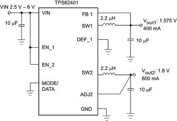
TPS6240x, Dual Outputs Step Down Converter
- 9.2.1.1 Design Requirements
- 9.2.1.2
Detailed Design Procedure
- 9.2.1.2.1 Converter1 Adjustable Default Output Voltage Setting: TPS62400
- 9.2.1.2.2 Converter1 Fixed Default Output Voltage Setting (TPS62401, TPS62402, TPS62403, TPS62404).
- 9.2.1.2.3 Converter 2 Adjustable Default Output Voltage Setting TPS62400:
- 9.2.1.2.4 Converter 2 Fixed Default Output Voltage Setting
- 9.2.1.2.5 Output Filter Design (Inductor and Output Capacitor)
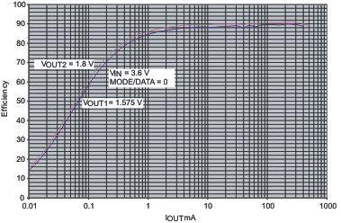
- 9.2.1.3 Application Curves
- 9.2.2 Various Output Voltages
- 9.2.3 Dynamic Voltage Scaling on Converter 1 by DEF_1 Pin
- 9.2.1
TPS6240x, Dual Outputs Step Down Converter
- 10Power Supply Recommendations
- 11Layout
- 12Device and Documentation Support
- 13Mechanical, Packaging, and Orderable Information
1 Features
- High Efficiency—Up to 95%
- VIN Range From 2.5 V to 6 V
- 2.25-MHz Fixed Frequency Operation
- Output Current of 400 mA and 600 mA
- Adjustable Output Voltage From 0.6V to VIN
- Pin-Selectable Output Voltage Supports Simple Dynamic Voltage Scaling
- EasyScale™ Optional One-Pin Serial Interface
- Power Save Mode at Light Load Currents
- 180° Out-of-Phase Operation
- Output Voltage Accuracy in PWM Mode ±1%
- Typical 32-μA Quiescent Current for Both Converters
- 100% Duty Cycle for Lowest Dropout
- Available in a 10-Pin VSON (3 mm × 3 mm)
2 Applications
- Cell Phones, Smart Phones
- PDAs, Pocket PCs
- OMAP™ and Low-Power DSP Supply
- Portable Media Players
- Digital Radios
- Digital Cameras
3 Description
The TPS6240x family of devices are synchronous dual step-down DC-DC converters optimized for battery-powered portable applications. The devices provide two independent output voltage rails powered by 1-cell Li-Ion or 3-cell NiMH/NiCD batteries. The devices are also suitable to operate from a standard 3.3-V or 5-V voltage rail.
With an input voltage range from 2.5 V to 6 V, the TPS6240x is ideal to power portable applications like smart phones, PDAs, and other portable equipment.
With the EasyScale serial interface the output voltages can be modified during operation. The fixed output voltage versions TPS62401, TPS62402, TPS62403, and TPS62404 support one-pin controlled simple Dynamic Voltage Scaling for low-power processors.
The TPS6240x operates at a 2.25-MHz fixed switching frequency and enters the power save mode operation at light load currents to maintain high efficiency over the entire load current range. For low noise applications the devices can be forced into fixed frequency PWM mode by pulling the MODE/DATA pin high. In the shutdown mode, the current consumption is reduced to 1.2 μA, typical. The devices allow the use of small inductors and capacitors to achieve a small solution size.
The TPS6240x is available in a 10-pin leadless package (3-mm × 3-mm VSON)
Device Information(1)
| PART NUMBER | PACKAGE | BODY SIZE (NOM) |
|---|---|---|
| TPS6240x | VSON (10) | 3.00 mm x 3.00 mm |
Simplified Schematic
Efficiency vs Output Current