SLVSAI5B September 2010 – June 2016 TPS62290-Q1 , TPS62293-Q1
UNLESS OTHERWISE NOTED, this document contains PRODUCTION DATA.
- 1 Features
- 2 Applications
- 3 Description
- 4 Revision History
- 5 Pin Configuration and Functions
- 6 Specifications
- 7 Parameter Measurement Information
- 8 Detailed Description
- 9 Application and Implementation
- 10Power Supply Recommendations
- 11Layout
- 12Device and Documentation Support
- 13Mechanical, Packaging, and Orderable Information
1 Features
- Qualified for Automotive Applications
- High Efficiency Step-Down Converter
- Output Current up to 1000 mA
- VIN Range From 2.3 V to 6 V
- 2.25-MHz Fixed Frequency Operation
- Power Save Mode at Light Load Currents
- Output Voltage Accuracy in PWM mode ±1.5%
- Fixed Output Voltage Options
- Typical 15-µA Quiescent Current
- 100% Duty Cycle for Lowest Dropout
- Voltage Positioning at Light Loads
- Available in a 2-mm × 2-mm × 0.8-mm SON Package
2 Applications
3 Description
The TPS6229x-Q1 is a highly efficient synchronous step-down buck converter optimized for automotive low input voltage applications, and provides up to 1000-mA output current..
With an input voltage range of 2.3 V to 6 V, and an output voltage accuracy of 1.5%, the device powers a large variety of automotive applications.
The TPS6229x-Q1 operates at 2.25-MHz fixed switching frequency and enters Power Save Mode operation with typical quiescent current of 15 µA at light load currents to maintain a high efficiency over the entire load current range.
The Power Save Mode is optimized for low output voltage ripple. For low noise applications, the device can be forced into fixed frequency PWM mode by pulling the MODE pin high. In the shutdown mode, the current consumption is reduced to less than 1 µA. The TPS6229x-Q1 allows the use of small inductors and capacitors to achieve a small solution size.
The TPS6229x-Q1 is available in a 2-mm × 2-mm
6-pin SON package.
Device Information(1)
| PART NUMBER | PACKAGE | BODY SIZE (NOM) |
|---|---|---|
| TPS6229x-Q1 | SON (6) | 2.00 mm × 2.00 mm |
- For all available packages, see the orderable addendum at the end of the data sheet.
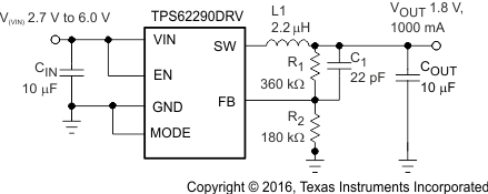
Typical Application Schematic

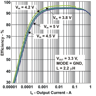
Efficiency vs Output Current
