SLUSAH4D MARCH 2011 – February 2016 TPS56121
PRODUCTION DATA.
- 1 Features
- 2 Applications
- 3 Description
- 4 Revision History
- 5 Pin Configuration and Functions
- 6 Specifications
-
7 Detailed Description
- 7.1 Overview
- 7.2 Functional Block Diagram
- 7.3 Feature Description
- 7.4 Device Functional Modes
-
8 Application and Implementation
- 8.1 Application Information
- 8.2
Typical Application
- 8.2.1 Design Requirements
- 8.2.2
Detailed Design Procedure
- 8.2.2.1 Switching Frequency Selection
- 8.2.2.2 Inductor Selection (L1)
- 8.2.2.3 Output Capacitor Selection
- 8.2.2.4 Inductor Peak Current Rating
- 8.2.2.5 Input Capacitor Selection
- 8.2.2.6 Bootstrap Capacitor (C14)
- 8.2.2.7 Bootstrap Resistor (R2)
- 8.2.2.8 RC Snubber (R9 and C18)
- 8.2.2.9 VDD Bypass Capacitor (C11)
- 8.2.2.10 BP5 Bypass Capacitor (C12)
- 8.2.2.11 Soft-Start Capacitor (C13)
- 8.2.2.12 Current Limit (R1)
- 8.2.2.13 Feedback Divider (R4, R7)
- 8.2.2.14 Compensation (C15, C16, C17, R3, R6)
- 8.2.3 Application Curves
- 9 Power Supply Recommendations
- 10Layout
- 11Device and Documentation Support
- 12Mechanical, Packaging, and Orderable Information
1 Features
- 4.5-V to 14-V Input Voltage Range
- Incorporates Power Block Technology
- Up to 15-A Output Current
- Fixed-Frequency Options of 300 kHz, 500 kHz, and 1 MHz
- High-Side and Low-Side MOSFET RDS(on) Sensing
- Programmable Soft-Start
- 600-mV Reference Voltage With 1% Accuracy
- Voltage Mode Control with Feed-Forward
- Supports Prebiased Output
- Thermal Shutdown
- 22-Pin 5-mm x 6-mm PQFN PowerPAD™ Package
- For SWIFT™ Power Products Documentation, see http://www.ti.com/swift
2 Applications
- Point-of-Load (POL) Power Modules
- High-Density DC-DC Converters for Telecom and Networking Applications
3 Description
The TPS56121 device is a high-efficiency and high-current synchronous buck converter designed to operate from a supply of 4.5 V to 14 V. The device can produce an output voltage as low as 0.6 V at loads up to 15 A. Integrated NexFET™ Power MOSFETs provide a small footprint and ease of use.
The device implements a voltage-mode control with voltage feed-forward compensation that responds instantly to input voltage change.
The TPS56121 is available in a thermally enhanced 22-pin PQFN (DQP) PowerPAD package.
The device offers design flexibility with a variety of user programmable functions, including soft-start, overcurrent protection (OCP) levels, and loop compensation. OCP levels are programmed by a single external resistor connected from the ILIM pin to the circuit ground. During the initial power-on sequence, the device enters a calibration cycle, measures the voltage at the ILIM pin, and sets an internal OCP voltage level. During operation, the programmed OCP voltage level is compared to the voltage drop across the low-side FET when it is on to determine whether there is an overcurrent condition and then enters a shutdown/restart cycle until the fault is removed.
Device Information(1)
| PART NUMBER | PACKAGE | BODY SIZE (NOM) |
|---|---|---|
| TPS56121 | LSON-CLIP (22) | 6.00 mm × 5.00 mm |
- For all available packages, see the orderable addendum at the end of the datasheet.
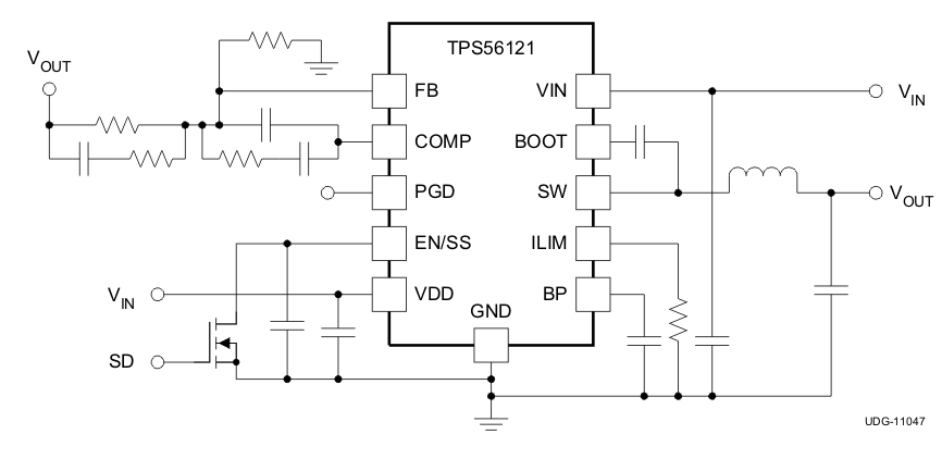
Simplified Application
