SLVS932F May 2009 – November 2014 TPS54325
PRODUCTION DATA.
- 1 Features
- 2 Applications
- 3 Description
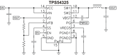
- 4 Simplified Schematic
- 5 Revision History
- 6 Pin Configuration and Functions
- 7 Specifications
- 8 Detailed Description
- 9 Application and Implementation
- 10Power Supply Recommendations
- 11Layout
- 12Device and Documentation Support
- 13Mechanical, Packaging, and Orderable Information
1 Features
- D-CAP2™ Mode Enables Fast Transient Response
- Low Output Ripple and Allows Ceramic Output Capacitor
- Wide VCC Input Voltage Range: 4.5 V to 18 V
- Wide VIN Input Voltage Range: 2.0 V to 18 V
- Output Voltage Range: 0.76 V to 5.5 V
- Highly Efficient Integrated FET’s Optimized for Lower Duty Cycle Applications – 120 mΩ (High Side) and 70 mΩ (Low Side)
- High Efficiency, less than 10 μA at shutdown
- High Initial Bandgap Reference Accuracy
- Adjustable Soft Start
- Pre-Biased Soft Start
- 700-kHz Switching Frequency (fSW)
- Cycle By Cycle Over Current Limit
- Power Good Output
2 Applications
- Wide Range of Applications for Low Voltage System
- Digital TV Power Supply
- High Definition Blu-ray Disc™ Players
- Networking Home Terminal
- Digital Set Top Box (STB)
3 Description
The TPS54325 device is an adaptive on-time D-CAP2™ mode synchronous buck converter. The TPS54325 device enables system designers to complete the suite of various end equipment’s power bus regulators with a cost effective, low component count, low standby current solution.
The main control loop for the TPS54325 uses the D-CAP2™ mode control which provides a very fast transient response with no external components. The TPS54325 also has a proprietary circuit that enables the device to adapt to both low equivalent series resistance (ESR) output capacitors, such as POSCAP or SP-CAP, and ultra-low ESR ceramic capacitors. The device operates from 4.5-V to 18-V VCC input , and from 2.0-V to 18-V VIN input power supply voltage. The output voltage can be programmed between 0.76 V and 5.5 V. The device also features an adjustable slow start time and a power good function. The TPS54325 is available in the 14 pin HTSSOP package, and designed to operate from –40°C to 85°C.
Device Information(1)
| PART NUMBER | PACKAGE | BODY SIZE (NOM) |
|---|---|---|
| TPS54325 | HTSSOP (14) | 5.00 mm × 4.40 mm |
- For all available packages, see the orderable addendum at the end of the datasheet.
4 Simplified Schematic
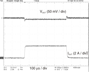
Load Transient Response