SLVSAU6H June 2011 – April 2016 TPS2000C , TPS2001C , TPS2041C , TPS2051C , TPS2061C , TPS2065C , TPS2065C-2 , TPS2068C , TPS2069C , TPS2069C-2
PRODUCTION DATA.
- 1 Features
- 2 Applications
- 3 Description
- 4 Revision History
- 5 Device Comparison Table
- 6 Pin Configuration and Functions
-
7 Specifications
- 7.1 Absolute Maximum Ratings
- 7.2 ESD Ratings
- 7.3 Recommended Operating Conditions
- 7.4 Thermal Information: SOT-23
- 7.5 Thermal Information: MSOP-PowerPAD
- 7.6 Electrical Characteristics: TJ = TA = 25°C
- 7.7 Electrical Characteristics: -40°C ≤ TJ ≤ 125°C
- 7.8 Timing Requirements: TJ = TA = 25°C
- 7.9 Typical Characteristics
- 8 Detailed Description
- 9 Application and Implementation
- 10Power Supply Recommendations
- 11Layout
- 12Device and Documentation Support
- 13Mechanical, Packaging, and Orderable Information
11 Layout
11.1 Layout Guidelines
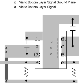
- Place the 100-nF bypass capacitor near the IN and GND pins, and make the connections using a low inductance trace.
- Place at least 10-µF low ESR ceramic capacitor near the OUT and GND pins, and make the connections using a low inductance trace.
- The PowerPAD must be directly connected to PCB ground plane using wide and short copper trace.
11.2 Layout Example
 Figure 42. Recommended Layout
11.3 Power Dissipation and Junction Temperature
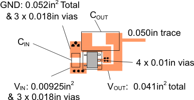
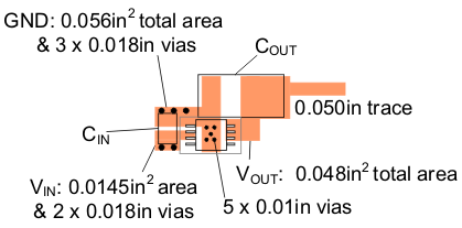
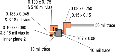
It is good design practice to estimate power dissipation and maximum expected junction temperature of the TPS20xxC and TPS20xxC-2. The system designer can control choices of package, proximity to other power dissipating devices, and printed-circuit board (PCB) design based on these calculations. These have a direct influence on maximum junction temperature. Other factors, such as airflow and maximum ambient temperature, are often determined by system considerations. It is important to remember that these calculations do not include the effects of adjacent heat sources, and enhanced or restricted air flow.
Addition of extra PCB copper area around these devices is recommended to reduce the thermal impedance and maintain the junction temperature as low as practical. The lower junction temperatures achieved by soldering the pad improve the efficiency and reliability of both TPS20xxC and TPS20xxC-2 parts and the system. The following examples were used to determine the θJACustom thermal impedances noted in Thermal Information: SOT-23 and Thermal Information: MSOP-PowerPAD. They were based on use of the JEDEC high-k circuit board construction (2 signal and 2 plane) with 4, 1-oz. copper weight, layers.
While TI recommends that the DGN package PAD be soldered to circuit board copper fill and vias for low thermal impedance, there may be cases where this is not desired. For example, use of routing area under the IC. Some devices are available in packages without the PowerPad (DGK) specifically for this purpose. The θJA for the DGN package with the pad not soldered and no extra copper, is approximately 141°C/W for 0.5-A and 1-A rated parts, and 139°C/W for the 1.5-A and 2-A rated parts. The θJA for the DGK mounted per Figure 45 is 110.3°C/W. These values may be used in Equation 1 to determine the maximum junction temperature.
 Figure 43. DBV Package PCB Layout Example
 Figure 44. DGN Package PCB Layout Example
 Figure 45. DGK Package PCB Layout Example
As shown in Equation 1, the following procedure requires iteration because power loss is due to the internal MOSFET I2 × RDS(ON), and RDS(ON) is a function of the junction temperature. As an initial estimate, use the RDS(ON) at 125°C from the Typical Characteristics, and the preferred package thermal resistance for the preferred board construction from the Thermal Information: SOT-23 table.
where
- IOUT = rated OUT pin current (A)
- RDS(ON) = Power switch ON-resistance at an assumed TJ (Ω)
- TA = Maximum ambient temperature (°C)
- TJ = Maximum junction temperature (°C)
- θJA = Thermal resistance (°C/W)
If the calculated TJ is substantially different from the original assumption, estimate a new value of RDS(ON) using the typical characteristic plot and recalculate.
If the resulting TJ is not less than 125°C, try a PCB construction or a package with lower θJA.