ZHCSQ93B March 2022 – December 2023 TMUX7236
PRODUCTION DATA
- 1
- 1 特性
- 2 应用
- 3 说明
- 4 Pin Configuration and Functions
-
5 Specifications
- 5.1 Absolute Maximum Ratings
- 5.2 ESD Ratings
- 5.3 Thermal Information
- 5.4 Recommended Operating Conditions
- 5.5 Source or Drain Continuous Current
- 5.6 ±15 V Dual Supply: Electrical Characteristics
- 5.7 ±15 V Dual Supply: Switching Characteristics
- 5.8 ±20 V Dual Supply: Electrical Characteristics
- 5.9 ±20 V Dual Supply: Switching Characteristics
- 5.10 44 V Single Supply: Electrical Characteristics
- 5.11 44 V Single Supply: Switching Characteristics
- 5.12 12 V Single Supply: Electrical Characteristics
- 5.13 12 V Single Supply: Switching Characteristics
- 5.14 Typical Characteristics
-
6 Parameter Measurement Information
- 6.1 On-Resistance
- 6.2 Off-Leakage Current
- 6.3 On-Leakage Current
- 6.4 Transition Time
- 6.5 tON(EN) and tOFF(EN)
- 6.6 Break-Before-Make
- 6.7 tON (VDD) Time
- 6.8 Propagation Delay
- 6.9 Charge Injection
- 6.10 Off Isolation
- 6.11 Crosstalk
- 6.12 Bandwidth
- 6.13 THD + Noise
- 6.14 Power Supply Rejection Ratio (PSRR)
- 7 Detailed Description
- 8 Application and Implementation
- 9 Device and Documentation Support
- 10Revision History
- 11Mechanical, Packaging, and Orderable Information
封装选项
请参考 PDF 数据表获取器件具体的封装图。
机械数据 (封装 | 引脚)
- PW|16
- RUM|16
散热焊盘机械数据 (封装 | 引脚)
- RUM|16
订购信息
7.2.7 Ultra-Low Charge Injection
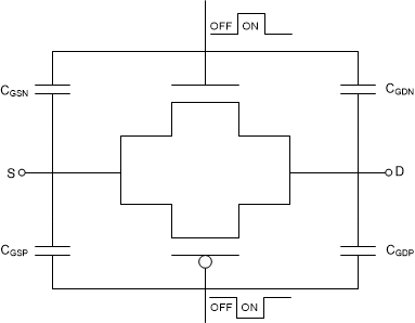
Figure 7-1 shows how the TMUX7236 device has a transmission gate topology. Any mismatch in the stray capacitance associated with the NMOS and PMOS causes an output level change whenever the switch is opened or closed.
 Figure 7-1 Transmission Gate Topology
The TMUX7236 contains specialized architecture to reduce charge injection on the Drain (Dx). To further reduce charge injection in a sensitive application, a compensation capacitor (Cp) can be added on the Source (Sx). This will push excess charge from the switch transition into the compensation capacitor on the Source (Sx) instead of the Drain (Dx). As a general rule, Cp should be 20x larger than the equivalent load capacitance on the Drain (Dx). Figure 7-2 shows charge injection variation with different compensation capacitors on the Source side. Figure 7-2 was captured on the TMUX7219 as part of the TMUX72xx family with a 100 pF load capacitance.
 Figure 7-2 Charge Injection
Compensation