ZHCSAH6F November   2012  – September 2021 TMS320F28050 , TMS320F28051 , TMS320F28052 , TMS320F28052F , TMS320F28052M , TMS320F28053 , TMS320F28054 , TMS320F28054F , TMS320F28054M , TMS320F28055

PRODUCTION DATA  

  1. 特性
  2. 应用
  3. 说明
    1. 3.1 功能方框图
  4. Revision History
  5. Device Comparison
    1. 5.1 Related Products
  6. Terminal Configuration and Functions
    1. 6.1 Pin Diagram
    2. 6.2 Signal Descriptions
      1. 6.2.1 Signal Descriptions
  7. Specifications
    1. 7.1  Absolute Maximum Ratings
    2. 7.2  ESD Ratings – Commercial
    3. 7.3  ESD Ratings – Automotive
    4. 7.4  Recommended Operating Conditions
    5. 7.5  Power Consumption Summary
      1. 7.5.1 TMS320F2805x Current Consumption at 60-MHz SYSCLKOUT
      2. 7.5.2 Reducing Current Consumption
      3. 7.5.3 Current Consumption Graphs (VREG Enabled)
    6. 7.6  Electrical Characteristics
    7. 7.7  Thermal Resistance Characteristics for PN Package
    8. 7.8  Thermal Design Considerations
    9. 7.9  JTAG Debug Probe Connection Without Signal Buffering for the MCU
    10. 7.10 Parameter Information
      1. 7.10.1 Timing Parameter Symbology
      2. 7.10.2 General Notes on Timing Parameters
    11. 7.11 Test Load Circuit
    12. 7.12 Power Sequencing
      1. 7.12.1 Reset ( XRS) Timing Requirements
      2. 7.12.2 Reset ( XRS) Switching Characteristics
    13. 7.13 Clock Specifications
      1. 7.13.1 Device Clock Table
        1. 7.13.1.1 2805x Clock Table and Nomenclature (60-MHz Devices)
        2. 7.13.1.2 Device Clocking Requirements/Characteristics
        3. 7.13.1.3 Internal Zero-Pin Oscillator (INTOSC1, INTOSC2) Characteristics
      2. 7.13.2 Clock Requirements and Characteristics
        1. 7.13.2.1 XCLKIN Timing Requirements - PLL Enabled
        2. 7.13.2.2 XCLKIN Timing Requirements - PLL Disabled
        3. 7.13.2.3 XCLKOUT Switching Characteristics (PLL Bypassed or Enabled)
    14. 7.14 Flash Timing
      1. 7.14.1 Flash/OTP Endurance for T Temperature Material
      2. 7.14.2 Flash/OTP Endurance for S Temperature Material
      3. 7.14.3 Flash/OTP Endurance for Q Temperature Material
      4. 7.14.4 Flash Parameters at 60-MHz SYSCLKOUT
      5. 7.14.5 Flash/OTP Access Timing
      6. 7.14.6 Flash Data Retention Duration
  8. Detailed Description
    1. 8.1 Overview
      1. 8.1.1  CPU
      2. 8.1.2  Control Law Accelerator
      3. 8.1.3  Memory Bus (Harvard Bus Architecture)
      4. 8.1.4  Peripheral Bus
      5. 8.1.5  Real-Time JTAG and Analysis
      6. 8.1.6  Flash
      7. 8.1.7  M0, M1 SARAMs
      8. 8.1.8  L0 SARAM, and L1, L2, and L3 DPSARAMs
      9. 8.1.9  Boot ROM
        1. 8.1.9.1 Emulation Boot
        2. 8.1.9.2 GetMode
        3. 8.1.9.3 Peripheral Pins Used by the Bootloader
      10. 8.1.10 Security
      11. 8.1.11 Peripheral Interrupt Expansion Block
      12. 8.1.12 External Interrupts (XINT1 to XINT3)
      13. 8.1.13 Internal Zero-Pin Oscillators, Oscillator, and PLL
      14. 8.1.14 Watchdog
      15. 8.1.15 Peripheral Clocking
      16. 8.1.16 Low-power Modes
      17. 8.1.17 Peripheral Frames 0, 1, 2, 3 (PFn)
      18. 8.1.18 General-Purpose Input/Output Multiplexer
      19. 8.1.19 32-Bit CPU-Timers (0, 1, 2)
      20. 8.1.20 Control Peripherals
      21. 8.1.21 Serial Port Peripherals
    2. 8.2 Memory Maps
    3. 8.3 Register Map
    4. 8.4 Device Emulation Registers
    5. 8.5 VREG, BOR, POR
      1. 8.5.1 On-chip VREG
        1. 8.5.1.1 Using the On-chip VREG
        2. 8.5.1.2 Disabling the On-chip VREG
      2. 8.5.2 On-chip Power-On Reset and Brownout Reset Circuit
    6. 8.6 System Control
      1. 8.6.1 Internal Zero-Pin Oscillators
      2. 8.6.2 Crystal Oscillator Option
      3. 8.6.3 PLL-Based Clock Module
      4. 8.6.4 Loss of Input Clock (NMI-watchdog Function)
      5. 8.6.5 CPU-watchdog Module
    7. 8.7 Low-power Modes Block
    8. 8.8 Interrupts
      1. 8.8.1 External Interrupts
        1. 8.8.1.1 External Interrupt Electrical Data/Timing
          1. 8.8.1.1.1 External Interrupt Timing Requirements
          2. 8.8.1.1.2 External Interrupt Switching Characteristics
    9. 8.9 Peripherals
      1. 8.9.1  Control Law Accelerator
        1. 8.9.1.1 CLA Device-Specific Information
        2. 8.9.1.2 CLA Register Descriptions
      2. 8.9.2  Analog Block
        1. 8.9.2.1 Analog-to-Digital Converter
          1. 8.9.2.1.1 ADC Device-Specific Information
          2. 8.9.2.1.2 ADC Electrical Data/Timing
            1. 8.9.2.1.2.1 ADC Electrical Characteristics
            2. 8.9.2.1.2.2 ADC Power Modes
            3. 8.9.2.1.2.3 External ADC Start-of-Conversion Electrical Data/Timing
              1. 8.9.2.1.2.3.1 External ADC Start-of-Conversion Switching Characteristics
            4. 8.9.2.1.2.4 Internal Temperature Sensor
              1. 8.9.2.1.2.4.1 Temperature Sensor Coefficient
            5. 8.9.2.1.2.5 ADC Power-Up Control Bit Timing
              1. 8.9.2.1.2.5.1 ADC Power-Up Delays
            6. 8.9.2.1.2.6 ADC Sequential and Simultaneous Timings
        2. 8.9.2.2 Analog Front End
          1. 8.9.2.2.1 AFE Device-Specific Information
          2. 8.9.2.2.2 AFE Register Descriptions
          3. 8.9.2.2.3 PGA Electrical Data/Timing
          4. 8.9.2.2.4 Comparator Block Electrical Data/Timing
            1. 8.9.2.2.4.1 Electrical Characteristics of the Comparator/DAC
          5. 8.9.2.2.5 VREFOUT Buffered DAC Electrical Data
            1. 8.9.2.2.5.1 Electrical Characteristics of VREFOUT Buffered DAC
      3. 8.9.3  Detailed Descriptions
      4. 8.9.4  Serial Peripheral Interface
        1. 8.9.4.1 SPI Device-Specific Information
        2. 8.9.4.2 SPI Register Descriptions
        3. 8.9.4.3 SPI Master Mode Electrical Data/Timing
          1. 8.9.4.3.1 SPI Master Mode External Timing (Clock Phase = 0)
          2. 8.9.4.3.2 SPI Master Mode External Timing (Clock Phase = 1)
        4. 8.9.4.4 SPI Slave Mode Electrical Data/Timing
          1. 8.9.4.4.1 SPI Slave Mode External Timing (Clock Phase = 0)
          2. 8.9.4.4.2 SPI Slave Mode External Timing (Clock Phase = 1)
      5. 8.9.5  Serial Communications Interface
        1. 8.9.5.1 SCI Device-Specific Information
        2. 8.9.5.2 SCI Register Descriptions
      6. 8.9.6  Enhanced Controller Area Network
        1. 8.9.6.1 eCAN Device-Specific Information
        2. 8.9.6.2 eCAN Register Descriptions
      7. 8.9.7  Inter-Integrated Circuit
        1. 8.9.7.1 I2C Device-Specific Information
        2. 8.9.7.2 I2C Register Descriptions
        3. 8.9.7.3 I2C Electrical Data/Timing
          1. 8.9.7.3.1 I2C Timing Requirements
          2. 8.9.7.3.2 I2C Switching Characteristics
      8. 8.9.8  Enhanced Pulse Width Modulator
        1. 8.9.8.1 ePWM Device-Specific Information
        2. 8.9.8.2 ePWM Register Descriptions
        3. 8.9.8.3 ePWM Electrical Data/Timing
          1. 8.9.8.3.1 ePWM Timing Requirements
          2. 8.9.8.3.2 ePWM Switching Characteristics
          3. 8.9.8.3.3 Trip-Zone Input Timing
            1. 8.9.8.3.3.1 Trip-Zone Input Timing Requirements
      9. 8.9.9  Enhanced Capture Module
        1. 8.9.9.1 eCAP Module Device-Specific Information
        2. 8.9.9.2 eCAP Module Register Descriptions
        3. 8.9.9.3 eCAP Module Electrical Data/Timing
          1. 8.9.9.3.1 eCAP Timing Requirement
          2. 8.9.9.3.2 eCAP Switching Characteristics
      10. 8.9.10 Enhanced Quadrature Encoder Pulse
        1. 8.9.10.1 eQEP Device-Specific Information
        2. 8.9.10.2 eQEP Register Descriptions
        3. 8.9.10.3 eQEP Electrical Data/Timing
          1. 8.9.10.3.1 eQEP Timing Requirements
          2. 8.9.10.3.2 eQEP Switching Characteristics
      11. 8.9.11 JTAG Port
        1. 8.9.11.1 JTAG Port Device-Specific Information
      12. 8.9.12 General-Purpose Input/Output
        1. 8.9.12.1 GPIO Device-Specific Information
        2. 8.9.12.2 GPIO Register Descriptions
        3. 8.9.12.3 GPIO Electrical Data/Timing
          1. 8.9.12.3.1 GPIO - Output Timing
            1. 8.9.12.3.1.1 General-Purpose Output Switching Characteristics
          2. 8.9.12.3.2 GPIO - Input Timing
            1. 8.9.12.3.2.1 General-Purpose Input Timing Requirements
          3. 8.9.12.3.3 Sampling Window Width for Input Signals
          4. 8.9.12.3.4 Low-Power Mode Wakeup Timing
            1. 8.9.12.3.4.1 IDLE Mode Timing Requirements
            2. 8.9.12.3.4.2 IDLE Mode Switching Characteristics
            3. 8.9.12.3.4.3 STANDBY Mode Timing Requirements
            4. 8.9.12.3.4.4 STANDBY Mode Switching Characteristics
            5. 8.9.12.3.4.5 HALT Mode Timing Requirements
            6. 8.9.12.3.4.6 HALT Mode Switching Characteristics
  9. Applications, Implementation, and Layout
    1. 9.1 TI Reference Design
  10. 10Device and Documentation Support
    1. 10.1 Getting Started
    2. 10.2 Device and Development Support Tool Nomenclature
    3. 10.3 Tools and Software
    4. 10.4 Documentation Support
    5. 10.5 支持资源
    6. 10.6 Trademarks
    7. 10.7 Electrostatic Discharge Caution
    8. 10.8 术语表
  11. 11Mechanical, Packaging, and Orderable Information
    1. 11.1 Packaging Information

封装选项

机械数据 (封装 | 引脚)
散热焊盘机械数据 (封装 | 引脚)
订购信息

Detailed Descriptions

Integral Nonlinearity

Integral nonlinearity refers to the deviation of each individual code from a line drawn from zero through full scale. The point used as zero occurs one-half LSB before the first code transition. The full-scale point is defined as level one-half LSB beyond the last code transition. The deviation is measured from the center of each particular code to the true straight line between these two points.

Differential Nonlinearity

An ideal ADC exhibits code transitions that are exactly 1 LSB apart. DNL is the deviation from this ideal value. A differential nonlinearity error of less than ±1 LSB ensures no missing codes.

Zero Offset

Zero error is the difference between the ideal input voltage and the actual input voltage that just causes a transition from an output code of zero to an output code of one.

Gain Error

The first code transition should occur at an analog value one-half LSB above negative full scale. The last transition should occur at an analog value one and one-half LSB below the nominal full scale. Gain error is the deviation of the actual difference between first and last code transitions and the ideal difference between first and last code transitions.

Signal-to-Noise Ratio + Distortion

Signal-to-noise ratio + distortion (SINAD) is the ratio of the rms value of the measured input signal to the rms sum of all other spectral components below the Nyquist frequency, including harmonics but excluding DC. The value for SINAD is expressed in decibels.

Effective Number of Bits

For a sine wave, SINAD can be expressed in terms of the number of bits. Using the formula GUID-40551D7E-68AD-4BDC-A03F-A751DBEF0C65-low.gif 
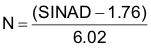
it is possible to get a measure of performance expressed as N, the effective number of bits (ENOB). Thus, the ENOB for a device for sine wave inputs at a given input frequency can be calculated directly from its measured SINAD.

Total Harmonic Distortion

Total harmonic distortion (THD) is the ratio of the rms sum of the first nine harmonic components to the rms value of the measured input signal and is expressed as a percentage or in decibels.

Spurious Free Dynamic Range

Spurious free dynamic range (SFDR) is the difference in dB between the rms amplitude of the input signal and the peak spurious signal.