SPRS377F September 2008 – June 2014 TMS320C6745 , TMS320C6747
PRODUCTION DATA.
- 1TMS320C6745, TMS320C6747 Fixed- and Floating-Point Digital Signal Processor
- 2Revision History
-
3Device Overview
- 3.1 Device Characteristics
- 3.2 Device Compatibility
- 3.3 DSP Subsystem
- 3.4 Memory Map Summary
- 3.5 Pin Assignments
- 3.6
Terminal Functions
- 3.6.1 Device Reset and JTAG
- 3.6.2 High-Frequency Oscillator and PLL
- 3.6.3 Real-Time Clock and 32-kHz Oscillator
- 3.6.4 External Memory Interface A (ASYNC, SDRAM)
- 3.6.5 External Memory Interface B (only SDRAM)
- 3.6.6 Serial Peripheral Interface Modules (SPI0, SPI1)
- 3.6.7 Enhanced Capture/Auxiliary PWM Modules (eCAP0, eCAP1, eCAP2)
- 3.6.8 Enhanced Pulse Width Modulators (eHRPWM0, eHRPWM1, eHRPWM2)
- 3.6.9 Enhanced Quadrature Encoder Pulse Module (eQEP)
- 3.6.10 Boot
- 3.6.11 Universal Asynchronous Receiver/Transmitters (UART0, UART1, UART2)
- 3.6.12 Inter-Integrated Circuit Modules (I2C0, I2C1)
- 3.6.13 Timers
- 3.6.14 Universal Host-Port Interface (UHPI)
- 3.6.15 Multichannel Audio Serial Ports (McASP0, McASP1, McASP2)
- 3.6.16 Universal Serial Bus Modules (USB0, USB1)
- 3.6.17 Ethernet Media Access Controller (EMAC)
- 3.6.18 Multimedia Card/Secure Digital (MMC/SD)
- 3.6.19 Liquid Crystal Display Controller (LCD)
- 3.6.20 General Purpose Input Output (GPIO)
- 3.6.21 Reserved and No Connect
- 3.6.22 Supply and Ground
- 3.6.23 Unused USB0 (USB2.0) and USB1 (USB1.1) Pin Configurations
- 4Device Configuration
-
5Device Operating Conditions
- 5.1 Absolute Maximum Ratings Over Operating Case Temperature Range (Unless Otherwise Noted)
- 5.2 Handling Ratings
- 5.3 Recommended Operating Conditions
- 5.4 Notes on Recommended Power-On Hours (POH)
- 5.5 Electrical Characteristics Over Recommended Ranges of Supply Voltage and Operating Case Temperature (Unless Otherwise Noted)
-
6Peripheral Information and Electrical Specifications
- 6.1 Parameter Information
- 6.2 Recommended Clock and Control Signal Transition Behavior
- 6.3 Power Supplies
- 6.4 Reset
- 6.5 Crystal Oscillator or External Clock Input
- 6.6 Clock PLLs
- 6.7 Interrupts
- 6.8 General-Purpose Input/Output (GPIO)
- 6.9 EDMA
- 6.10 External Memory Interface A (EMIFA)
- 6.11 External Memory Interface B (EMIFB)
- 6.12 Memory Protection Units
- 6.13 MMC / SD / SDIO (MMCSD)
- 6.14 Ethernet Media Access Controller (EMAC)
- 6.15 Management Data Input/Output (MDIO)
- 6.16 Multichannel Audio Serial Ports (McASP0, McASP1, and McASP2)
- 6.17
Serial Peripheral Interface Ports (SPI0, SPI1)
- 6.17.1 SPI Peripheral Registers Description(s)
- 6.17.2
SPI Electrical Data/Timing
- 6.17.2.1
Serial Peripheral Interface (SPI) Timing
- Table 6-54 General Timing Requirements for SPI0 Master Modes
- Table 6-55 General Timing Requirements for SPI0 Slave Modes
- Table 6-56 Additional SPI0 Master Timings, 4-Pin Enable Option
- Table 6-57 Additional SPI0 Master Timings, 4-Pin Chip Select Option
- Table 6-58 Additional SPI0 Master Timings, 5-Pin Option
- Table 6-59 Additional SPI0 Slave Timings, 4-Pin Enable Option
- Table 6-60 Additional SPI0 Slave Timings, 4-Pin Chip Select Option
- Table 6-61 Additional SPI0 Slave Timings, 5-Pin Option
- Table 6-62 General Timing Requirements for SPI1 Master Modes
- Table 6-63 General Timing Requirements for SPI1 Slave Modes
- Table 6-64 Additional SPI1 Master Timings, 4-Pin Enable Option
- Table 6-65 Additional SPI1 Master Timings, 4-Pin Chip Select Option
- Table 6-66 Additional SPI1 Master Timings, 5-Pin Option
- Table 6-67 Additional SPI1 Slave Timings, 4-Pin Enable Option
- Table 6-68 Additional SPI1 Slave Timings, 4-Pin Chip Select Option
- Table 6-69 Additional SPI1 Slave Timings, 5-Pin Option
- 6.17.2.1
Serial Peripheral Interface (SPI) Timing
- 6.18 Enhanced Capture (eCAP) Peripheral
- 6.19 Enhanced Quadrature Encoder (eQEP) Peripheral
- 6.20 Enhanced High-Resolution Pulse-Width Modulator (eHRPWM)
- 6.21 LCD Controller
- 6.22 Timers
- 6.23 Inter-Integrated Circuit Serial Ports (I2C0, I2C1)
- 6.24 Universal Asynchronous Receiver/Transmitter (UART)
- 6.25 USB1 Host Controller Registers (USB1.1 OHCI)
- 6.26 USB0 OTG (USB2.0 OTG)
- 6.27 Host-Port Interface (UHPI)
- 6.28 Power and Sleep Controller (PSC)
- 6.29 Programmable Real-Time Unit Subsystem (PRUSS)
- 6.30 Emulation Logic
- 6.31 IEEE 1149.1 JTAG
- 6.32 Real Time Clock (RTC)
- 7Device and Documentation Support
- 8Mechanical Packaging and Orderable Information
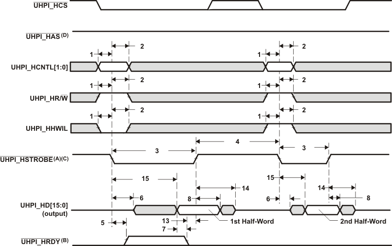
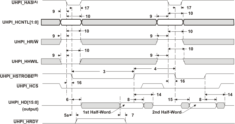
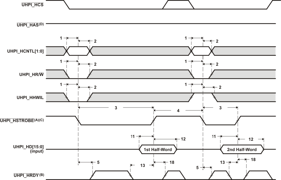
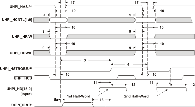
Table 6-100 Switching Characteristics for Host-Port Interface Cycles(1)(2)(3)
| No. | PARAMETER | MIN | MAX | UNIT | ||
|---|---|---|---|---|---|---|
| 5 | td(HSTBL-HRDYV) | Delay time,
UHPI_HSTROBE low to UHPI_HRDY valid |
For HPI Write, UHPI_HRDY can go high (not ready) for these HPI Write conditions; otherwise, UHPI_HRDY stays low (ready):
Case 1: Back-to-back HPIA writes (can be either first or second half-word) Case 2: HPIA write following a PREFETCH command (can be either first or second half-word) Case 3: HPID write when FIFO is full or flushing (can be either first or second half-word) Case 4: HPIA write and Write FIFO not empty For HPI Read, UHPI_HRDY can go high (not ready) for these HPI Read conditions: Case 1: HPID read (with auto-increment) and data not in Read FIFO (can only happen to first half-word of HPID access) Case 2: First half-word access of HPID Read without auto-increment For HPI Read, UHPI_HRDY stays low (ready) for these HPI Read conditions: Case 1: HPID read with auto-increment and data is already in Read FIFO (applies to either half-word of HPID access) Case 2: HPID read without auto-increment and data is already in Read FIFO (always applies to second half-word of HPID access) Case 3: HPIC or HPIA read (applies to either half-word access) |
12 | ns | |
| 5a | td(HASL-HRDYV) | Delay time, UHPI_HAS low to UHPI_HRDY valid | 13 | |||
| 6 | ten(HSTBL-HDLZ) | Enable time, HD driven from UHPI_HSTROBE low | 2 | ns | ||
| 7 | td(HRDYL-HDV) | Delay time, UHPI_HRDY low to HD valid | 0 | ns | ||
| 8 | toh(HSTBH-HDV) | Output hold time, HD valid after UHPI_HSTROBE high | 1.5 | ns | ||
| 14 | tdis(HSTBH-HDHZ) | Disable time, HD high-impedance from UHPI_ HSTROBE high | 12 | ns | ||
| 15 | td(HSTBL-HDV) | Delay time,
UHPI_HSTROBE low to HD valid |
For HPI Read. Applies to conditions where data is already residing in HPID/FIFO:
Case 1: HPIC or HPIA read Case 2: First half-word of HPID read with auto-increment and data is already in Read FIFO Case 3: Second half-word of HPID read with or without auto-increment |
15 | ns | |
| 18 | td(HSTBH-HRDYV) | Delay time,
UHPI_HSTROBE high to UHPI_HRDY valid |
For HPI Write, UHPI_HRDY can go high (not ready) for these HPI Write conditions; otherwise, UHPI_HRDY stays low (ready):
Case 1: HPID write when Write FIFO is full (can happen to either half-word) Case 2: HPIA write (can happen to either half-word) Case 3: HPID write without auto-increment (only happens to second half-word) |
12 | ns | |
(1) M=SYSCLK2 period (CPU clock frequency)/2 in ns.
(2) UHPI_HSTROBE refers to the following logical operation on UHPI_HCS, UHPI_HDS1, and UHPI_HDS2: [NOT(UHPI_HDS1 XOR UHPI_HDS2)] OR UHPI_HCS.
(3) By design, whenever UHPI_HCS is driven inactive (high), HPI will drive UHPI_HRDY active (low).

A. UHPI_HSTROBE refers to the following logical operation on UHPI_HCS, UHPI_HDS1, and UHPI_HDS2: [NOT(UHPI_HDS1 XOR UHPI_HDS2)] OR UHPI_HCS.
B. Depending on the type of write or read operation (HPID without auto-incrementing; HPIA, HPIC, or HPID with auto-incrementing) and the state of the FIFO, transitions on UHPI_HRDY may or may not occur.
C. UHPI_HCS reflects typical UHPI_HCS behavior when UHPI_HSTROBE assertion is caused by UHPI_HDS1 or UHPI_HDS2. UHPI_HCS timing requirements are reflected by parameters for UHPI_HSTROBE.
D. The diagram above assumes UHPI_HAS has been pulled high.
Figure 6-67 UHPI Read Timing (UHPI_HAS Not Used, Tied High) 
A. For correct operation, strobe the UHPI_HAS signal only once per UHPI_HSTROBE active cycle.
B. UHPI_HSTROBE refers to the following logical operation on UHPI_HCS, UHPI_HDS1, and UHPI_HDS2: [NOT(UHPI_HDS1 XOR UHPI_HDS2)] OR UHPI_HCS.
Figure 6-68 UHPI Read Timing (UHPI_HAS Used) 
A. UHPI_HSTROBE refers to the following logical operation on UHPI_HCS, UHPI_HDS1, and UHPI_HDS2: [NOT(UHPI_HDS1 XOR UHPI_HDS2)] OR UHPI_HCS.
B. Depending on the type of write or read operation (HPID without auto-incrementing; HPIA, HPIC, or HPID with auto-incrementing) and the state of the FIFO, transitions on UHPI_HRDY may or may not occur.
C. UHPI_HCS reflects typical UHPI_HCS behavior when UHPI_HSTROBE assertion is caused by UHPI_HDS1 or UHPI_HDS2. UHPI_HCS timing requirements are reflected by parameters for UHPI_HSTROBE.
D. he diagram above assumes UHPI_HAS has been pulled high.
Figure 6-69 UHPI Write Timing (UHPI_HAS Not Used, Tied High) 
A. For correct operation, strobe the UHPI_HAS signal only once per UHPI_HSTROBE active cycle.
B. UHPI_HSTROBE refers to the following logical operation on UHPI_HCS, UHPI_HDS1, and UHPI_HDS2: [NOT(UHPI_HDS1 XOR UHPI_HDS2)] OR UHPI_HCS.
Figure 6-70 UHPI Write Timing (UHPI_HAS Used)