请参考 PDF 数据表获取器件具体的封装图。
The TL77xxA family of integrated-circuit supply-voltage supervisors is designed specifically for use as reset controllers in microcomputer and microprocessor systems. The supply-voltage supervisor monitors the supply for undervoltage conditions at the SENSE input. During power up, the RESET output becomes active (low) when VCC attains a value approaching 3.6 V. At this point (assuming that SENSE is above VIT+), the delay timer function activates a time delay, after which outputs RESET and RESET go inactive (high and low, respectively). When an undervoltage condition occurs during normal operation, RESET and RESET go active.
PART NUMBER | PACKAGE | BODY SIZE (NOM) |
---|---|---|
TL77xxA | SOIC (8) | 4.90 mm × 3.91 mm |
PDIP (8) | 9.81 mm × 6.35 mm | |
TL7705A | SO (8) | 6.20 mm × 5.30 mm |
Changes from J Revision (January 2015) to K Revision
Changes from I Revision (July 2009) to J Revision
PIN | TYPE | DESCRIPTION | |
---|---|---|---|
NAME | NO. | ||
CT | 3 | I/O | External timing-capacitor pin |
GND | 4 | — | Device ground |
REF | 1 | O | Voltage reference output |
RESET | 6 | O | Supervisor reset signal output |
RESET | 5 | O | Supervisor reset signal output (inverted) |
RESIN | 2 | I | Reset input |
SENSE | 7 | I | Sense input |
VCC | 8 | — | Power Supply |
MIN | MAX | UNIT | |||
---|---|---|---|---|---|
VCC | Supply voltage(3) | 20 | V | ||
VI | Input voltage, RESIN | –0.3 | 20 | V | |
VI | Input voltage range SENSE | TL7702A(2) | –0.3 | 6 | V |
TL7705A | –0.3 | 20 | V | ||
TL7709A | –0.3 | 20 | V | ||
TL7712A, TL7715A | –0.3 | 20 | V | ||
IOH | High-level output current, IOH, RESET | –30 | mA | ||
IOL | Low-level output current, IOL, RESET | 30 | mA | ||
TJ | Operating virtual junction temperature | 150 | °C | ||
Tstg | Storage temperature | –65 | 150 | °C |
VALUE | UNIT | |||
---|---|---|---|---|
V(ESD) | Electrostatic discharge | Human body model (HBM), per ANSI/ESDA/JEDEC JS-001(1) | 1000 | V |
Charged device model (CDM), per JEDEC specification JESD22-C101(2) | 1000 |
MIN | MAX | UNIT | |||
---|---|---|---|---|---|
VCC | Supply Voltage | 3.5 | 18 | V | |
VIH | High-level input voltage at RESIN | 2 | V | ||
VIL | Low-level input voltage at RESIN | 0.6 | V | ||
VI | Input voltage, SENSE | TL7702A | 0 | See(1) | V |
TL7705A | 0 | 10 | |||
TL7709A | 0 | 15 | |||
TL7712A | 0 | 20 | |||
TL7715A | 0 | 20 | |||
IOH | High-level output current, RESET | –16 | mA | ||
IOL | Low-level output current, RESET | 16 | mA | ||
TA | Operating free-air temperature | TL77xxAC | 0 | 70 | °C |
TL77xxAI | –40 | 85 |
THERMAL METRIC(1) | TL77xxA | UNIT | |||
---|---|---|---|---|---|
D | P | PS | |||
8 PINS | 8 PINS | 8 PINS | |||
RθJA | Junction-to-ambient thermal resistance | 97 | 85 | 95 | °C/W |
PARAMETER | TEST CONDITIONS(1) | TL77xxAC TL77xxAI |
UNIT | ||||||
---|---|---|---|---|---|---|---|---|---|
MIN | TYP | MAX | |||||||
VOH | High-level output voltage, RESET | IOH = –16 mA | VCC – 1.5 | V | |||||
VOL | Low-level output voltage, RESET | IOL = 16 mA | 0.4 | V | |||||
Vref | Reference Voltage | TA = 25°C | 2.48 | 2.53 | 2.58 | V | |||
VIT– | Negative-going input threshold voltage, SENSE | TL7702A | TA = 25°C | 2.48 | 2.53 | 2.58 | V | ||
TL7705A | 4.5 | 4.55 | 4.6 | ||||||
TL7709A | 7.5 | 7.6 | 7.7 | ||||||
TL7712A | 10.6 | 10.8 | 11 | ||||||
TL7715A | 13.2 | 13.5 | 13.8 | ||||||
Vhys | Hysteresis, SENS (VIT+ – VIT–) | TL7702A | TA = 25°C | 10 | mV | ||||
TL7705A | 15 | ||||||||
TL7709A | 20 | ||||||||
TL7712A | 35 | ||||||||
TL7715A | 45 | ||||||||
II | Input current | RESIN | VI = 2.4 V to VCC | 20 | µA | ||||
VI = 0.4 V | –100 | ||||||||
SENSE | TL7702A | Vref < VI < VCC – 1.5 V | 0.5 | 2 | |||||
IOH | High-level output current, RESET | VO = 18 V | 50 | µA | |||||
IOL | Low-level output current, RESET | VO = 0 | –50 | µA | |||||
ICC | Supply current | All inputs and outputs open | 1.8 | 3 | mA |
PARAMETER | TEST CONDITIONS(1) | TL77xxAC TL77xxAI |
UNIT | ||||
---|---|---|---|---|---|---|---|
MIN | TYP | MAX | |||||
Output pulse duration | CT = 0.1 µF | 0.65 | 1.2 | 2.6 | msec | ||
Input pulse duration at RESIN | 0.4 | µs | |||||
tw(S) | Pulse duration at sense input to switch outputs | VIH = VIT− + 200 mV, VIL = VIT− − 200 mV | 2 | µs | |||
tpd | propagation delay time, RESIN to RESET | VCC = 5V | 1 | µs | |||
tr | Rise time | RESET | VCC = 5 V(2) | 0.2 | µs | ||
RESET | 3.5 | ||||||
tf | Fall time | RESET | VCC = 5 V(2) | 3.5 | µs | ||
RESET | 0.2 |
The TL77xxA family of integrated-circuit supply-voltage supervisors is designed specifically for use as reset controllers in microcomputer and microprocessor systems. The supply-voltage supervisor monitors the supply for undervoltage conditions at the SENSE input. During power up, the RESET output becomes active (low) when VCC attains a value approaching 3.6 V. At this point (assuming that SENSE is above VIT+), the delay timer function activates a time delay, after which outputs RESET and RESET go inactive (high and low, respectively). When an undervoltage condition occurs during normal operation, RESET and RESET go active. To ensure that a complete reset occurs, the reset outputs remain active for a time delay after the voltage at the SENSE input exceeds the positive-going threshold value.
During power down and when SENSE is below VIT−, the outputs remain active until VCC falls below 2 V. After this, the outputs are undefined. An external capacitor (typically 0.1 μF) must be connected to REF to reduce the influence of fast transients in the supply voltage.
Five versions of this circuit are available:
The functional block diagram is shown for illustrative purposes only; the actual circuit includes a trimming network to adjust the reference voltage and sense-comparator trip point.
Th TL77xxA family operates of a wide supply voltage range of 3.5 V to 18 V.
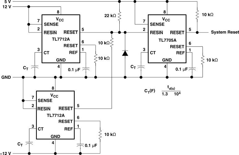
The time delay is determined by the value of the external capacitor CT: td = 1.3 × 10⁴ × CT, where CT is in farads (F) and td is in seconds (s).
The series TL77xxA incorporates an extremely stable reference voltage source. This voltage source can also be used in applications where a constant voltage source is required. The reference voltage varies less than 10 mV over the supply voltage range of 3.5 V to 18 V. The same stability of the reference voltage is maintained, when the ambient temperature is changed. The reference's voltage varies only 16 mV when the ambient temperature is changed from –40°C to +85°C.
Figure 7 shows the timing of the various signals. In this example the SENSE input is connected to the supply voltage VCC as in typical applications of this device. The minimum supply voltage for which the function of this device is guaranteed is 3.6 V. After power-on, the outputs are undefined until the minimum supply voltage Vres is reached. For the TL77xxA the minimum supply voltage is Vres = 3 V (typical 2.5 V). Beyond the voltage Vres the capacitor CT is first kept discharged, and the outputs stay in the active state (RESET = High, RESET = Low). When the input voltage becomes higher than the threshold voltage Vt, the thyristor is turned off and the capacitor is charged. After a delay, td, the voltage at the capacitor passes the trigger level of the output comparator and the outputs become inactive. The circuit to be initialized is now set to a defined state and starts the correct operation.
NOTE
Information in the following applications sections is not part of the TI component specification, and TI does not warrant its accuracy or completeness. TI’s customers are responsible for determining suitability of components for their purposes. Customers should validate and test their design implementation to confirm system functionality.
This application shows the initialization circuit diagrams for a microprocessor system with supply voltage Vcc = 5 V. The external components required are the decoupling capacitor Cref for the reference voltage and the timing capacitor CT. The outputs of the TL77xxA are open collector outputs. In Figure 8 therefore a pull-up resistor is shown at the RESET output to ensure the correct HIGH level.
The TL77xxA devices operate within the specifications from the Recommended Operating Conditions between 3.5 V and 18 V.
CAUTION
These devices risk being damaged when powered by more than 20 V.
The voltage monitor should be placed on the printed circuit board, where there are no neighboring circuits in the which switch high currents (like bus interface circuits and power switches). When laying out the layout of the printed circuit board, take special care with the interconnects which carry analog signals. Beside the SENSE input these are the CT and Vref terminals. Noise coupled into the CT input will lead to a reduction of the output pulse width. Noise coupled into the Vref input or into the filter capacitor at this input may lead to undesired triggering of the circuit and by this to an undesired RESET pulse. Practice shows, that this malfunction when high currents flow over the interconnects of these capacitors to the GND terminal of the voltage monitor. To avoid these effects, the GND terminals of these capacitors must be connected by the shortest way to the GND terminal of the voltage monitor in so that no currents caused by other circuits flow over these wires. Figure 16 show a layout proposal for the printed circuit board. Furthermore the resistors of the voltage divider at the SENSE input of the TL7702 (R2 and R3 in Figure 16) have to be placed in so, that no noise may be coupled into this circuit.
The table below lists quick access links. Categories include technical documents, support and community resources, tools and software, and quick access to sample or buy.
PARTS | PRODUCT FOLDER | SAMPLE & BUY | TECHNICAL DOCUMENTS | TOOLS & SOFTWARE | SUPPORT & COMMUNITY |
---|---|---|---|---|---|
TL7702A | Click here | Click here | Click here | Click here | Click here |
TL7705A | Click here | Click here | Click here | Click here | Click here |
TL7709A | Click here | Click here | Click here | Click here | Click here |
TL7712A | Click here | Click here | Click here | Click here | Click here |
TL7715A | Click here | Click here | Click here | Click here | Click here |
To receive notification of documentation updates, navigate to the device product folder on ti.com. In the upper right corner, click on Alert me to register and receive a weekly digest of any product information that has changed. For change details, review the revision history included in any revised document.
The following links connect to TI community resources. Linked contents are provided "AS IS" by the respective contributors. They do not constitute TI specifications and do not necessarily reflect TI's views; see TI's Terms of Use.
E2E is a trademark of Texas Instruments.
All other trademarks are the property of their respective owners.
This integrated circuit can be damaged by ESD. Texas Instruments recommends that all integrated circuits be handled with appropriate precautions. Failure to observe proper handling and installation procedures can cause damage.
ESD damage can range from subtle performance degradation to complete device failure. Precision integrated circuits may be more susceptible to damage because very small parametric changes could cause the device not to meet its published specifications.
SLYZ022 — TI Glossary.
This glossary lists and explains terms, acronyms, and definitions.
The following pages include mechanical, packaging, and orderable information. This information is the most current data available for the designated devices. This data is subject to change without notice and revision of this document. For browser-based versions of this data sheet, refer to the left-hand navigation.
Texas Instruments Incorporated and its subsidiaries (TI) reserve the right to make corrections, enhancements, improvements and other changes to its semiconductor products and services per JESD46, latest issue, and to discontinue any product or service per JESD48, latest issue. Buyers should obtain the latest relevant information before placing orders and should verify that such information is current and complete. All semiconductor products (also referred to herein as "components") are sold subject to TI's terms and conditions of sale supplied at the time of order acknowledgment.
TI warrants performance of its components to the specifications applicable at the time of sale, in accordance with the warranty in TI's terms and conditions of sale of semiconductor products. Testing and other quality control techniques are used to the extent TI deems necessary to support this warranty. Except where mandated by applicable law, testing of all parameters of each component is not necessarily performed.
TI assumes no liability for applications assistance or the design of Buyers' products. Buyers are responsible for their products and applications using TI components. To minimize the risks associated with Buyers' products and applications, Buyers should provide adequate design and operating safeguards.
TI does not warrant or represent that any license, either express or implied, is granted under any patent right, copyright, mask work right, or other intellectual property right relating to any combination, machine, or process in which TI components or services are used. Information published by TI regarding third-party products or services does not constitute a license to use such products or services or a warranty or endorsement thereof. Use of such information may require a license from a third party under the patents or other intellectual property of the third party, or a license from TI under the patents or other intellectual property of TI.
Reproduction of significant portions of TI information in TI data books or data sheets is permissible only if reproduction is without alteration and is accompanied by all associated warranties, conditions, limitations, and notices. TI is not responsible or liable for such altered documentation. Information of third parties may be subject to additional restrictions.
Resale of TI components or services with statements different from or beyond the parameters stated by TI for that component or service voids all express and any implied warranties for the associated TI component or service and is an unfair and deceptive business practice. TI is not responsible or liable for any such statements.
Buyer acknowledges and agrees that it is solely responsible for compliance with all legal, regulatory and safety-related requirements concerning its products, and any use of TI components in its applications, notwithstanding any applications-related information or support that may be provided by TI. Buyer represents and agrees that it has all the necessary expertise to create and implement safeguards which anticipate dangerous consequences of failures, monitor failures and their consequences, lessen the likelihood of failures that might cause harm and take appropriate remedial actions. Buyer will fully indemnify TI and its representatives against any damages arising out of the use of any TI components in safety-critical applications.
In some cases, TI components may be promoted specifically to facilitate safety-related applications. With such components, TI's goal is to help enable customers to design and create their own end-product solutions that meet applicable functional safety standards and requirements. Nonetheless, such components are subject to these terms.
No TI components are authorized for use in FDA Class III (or similar life-critical medical equipment) unless authorized officers of the parties have executed a special agreement specifically governing such use.
Only those TI components which TI has specifically designated as military grade or "enhanced plastic" are designed and intended for use in military/aerospace applications or environments. Buyer acknowledges and agrees that any military or aerospace use of TI components which have not been so designated is solely at the Buyer's risk, and that Buyer is solely responsible for compliance with all legal and regulatory requirements in connection with such use.
TI has specifically designated certain components as meeting ISO/TS16949 requirements, mainly for automotive use. In any case of use of non-designated products, TI will not be responsible for any failure to meet ISO/TS16949.
TI E2E Community : e2e.ti.com
Mailing Address: Texas Instruments, Post Office Box 655303, Dallas, Texas 75265
Copyright© 2016, Texas Instruments Incorporated