SBOS458H December 2008 – June 2015 THS4521 , THS4522 , THS4524
PRODUCTION DATA.
- 1 Features
- 2 Applications
- 3 Description
- 4 Revision History
- 5 Device Comparison Table
- 6 Pin Configuration and Functions
-
7 Specifications
- 7.1 Absolute Maximum Ratings
- 7.2 ESD Ratings
- 7.3 Recommended Operating Conditions
- 7.4 Thermal Information
- 7.5 Electrical Characteristics: VS+ - VS- = 3.3 V
- 7.6 Electrical Characteristics: VS+ - VS- = 5 V
- 7.7 Typical Characteristics
- 7.8 Typical Characteristics: VS+ - VS- = 3.3 V
- 7.9 Typical Characteristics: 5 V
-
8 Detailed Description
- 8.1 Overview
- 8.2 Functional Block Diagram
- 8.3
Feature Description
- 8.3.1 Frequency Response
- 8.3.2 Distortion
- 8.3.3 Slew Rate, Transient Response, Settling Time, Output Impedance, Overdrive, Output Voltage, and Turn-On/Turn-Off Time
- 8.3.4 Common-Mode and Power-Supply Rejection
- 8.3.5 VOCM Input
- 8.3.6 Typical Performance Variation With Supply VoltageTypical Performance Variation with Supply Voltage section
- 8.3.7 title of Single-Supply Operation sectionSingle-Supply Operation
- 8.3.8 Low-Power Applications and the Effects of Resistor Values on Bandwidth
- 8.3.9 Frequency Response Variation due to Package Options
- 8.3.10 Driving Capacitive Loads
- 8.3.11 Audio Performance
- 8.3.12 Audio On/Off Pop Performance
- 8.4
Device Functional Modes
- 8.4.1
Operation from Single-Ended Sources to Differential Outputs
- 8.4.1.1 AC-Coupled Signal Path Considerations for Single-Ended Input to Differential Output Conversion
- 8.4.1.2 DC-Coupled Input Signal Path Considerations for Single-Ended to Differential Conversion
- 8.4.1.3 Resistor Design Equations for the Single-Ended to Differential Configuration of the FDA
- 8.4.1.4 Input Impedance for the Single-Ended to Differential FDA Configuration
- 8.4.2 Differential-Input to Differential-Output Operation
- 8.4.1
Operation from Single-Ended Sources to Differential Outputs
- 8.5 Programming
-
9 Application and Implementation
- 9.1 Application Information
- 9.2 Typical Applications
- 10Power Supply Recommendations
- 11Layout
- 12Device and Documentation Support
- 13Mechanical, Packaging, and Orderable Information
1 Features
- Fully Differential Architecture
- Bandwidth: 145 MHz (AV = 1 V/V)
- Slew Rate: 490 V/μs
- HD2: –133 dBc at 10 kHz (1 VRMS, RL = 1 kΩ)
- HD3: –141 dBc at 10 kHz (1 VRMS, RL = 1 kΩ)
- Input Voltage Noise: 4.6 nV/√Hz (f = 100 kHz)
- THD+N: –112dBc (0.00025%) at 1 kHz (22-kHz BW, G = 1, 5 VPP)
- Open-Loop Gain: 119 dB (DC)
- NRI—Negative Rail Input
- RRO—Rail-to-Rail Output
- Output Common-Mode Control (with Low Offset)
- Power Supply:
- Power-Down Capability: 20 μA (typical)
2 Applications
3 Description
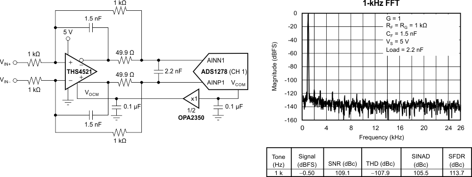
The THS4521, THS4522, and THS4524 family of devices are very low-power, fully differential amplifiers with rail-to-rail output and an input common-mode range that includes the negative rail. These amplifiers are designed for low-power data acquisition systems and high-density applications where power dissipation is a critical parameter, and provide exceptional performance in audio applications.
The family includes single FDA (THS4521), dual FDA (THS4522), and quad FDA (THS4524) versions.
Device Information(1)
| PART NUMBER | PACKAGE | BODY SIZE (NOM) |
|---|---|---|
| THS4521 | SOIC (8) | 4.90 mm × 3.91 mm |
| VSSOP (8) | 3.00 mm × 3.00 mm | |
| THS4522 | TSSOP (16) | 5.00 mm × 4.40 mm |
| THS4524 | TSSOP (38) | 9.70 mm × 4.40 mm |
- For all available packages, see the package option addendum at the end of the datasheet.
