ZHCSPG0 December 2021 TCAN1167-Q1
PRODUCTION DATA
- 1 特性
- 2 应用
- 3 说明
- 4 Revision History
- 5 说明(续)
- 6 Pin Configurations and Functions
- 7 Specifications
- 8 Parameter Measurement Information
-
9 Detailed Description
- 9.1 Overview
- 9.2 Functional Block Diagram
- 9.3
Feature Description
- 9.3.1 VSUP Pin
- 9.3.2 VCCOUT Pin
- 9.3.3 Digital Inputs and Outputs
- 9.3.4 GND
- 9.3.5 INH Pin
- 9.3.6 WAKE Pin
- 9.3.7 nRST Pin
- 9.3.8 SDO
- 9.3.9 nCS Pin
- 9.3.10 SCLK
- 9.3.11 SDI
- 9.3.12 CAN Bus Pins
- 9.3.13 Local Faults
- 9.3.14 Watchdog
- 9.3.15 Bus Fault Detection and Communication
- 9.4 Device Functional Modes
- 9.5
Programming
- 9.5.1 Serial Peripheral Interface (SPI) Communication
- 9.5.2 Serial Clock Input (SCLK)
- 9.5.3 Serial Data Input (SDI)
- 9.5.4 Serial Data Output (SDO)
- 9.5.5 Chip Select Not (nCS)
- 9.5.6
Registers
- 9.5.6.1 DEVICE_ID_y Register (Address = 0h + formula) [reset = xxh]
- 9.5.6.2 REV_ID_MAJOR Register (Address = 8h) [reset = 00h]
- 9.5.6.3 REV_ID_MINOR Register (Address = 9h) [reset = 00h]
- 9.5.6.4 SPI_RSVD_x Register (Address = Ah + formula) [reset = 00h]
- 9.5.6.5 Scratch_Pad_SPI Register (Address = Fh) [reset = 00h]
- 9.5.6.6 MODE_CNTRL Register (Address = 10h) [reset = 04h]
- 9.5.6.7 WD_CONFIG_1 Register (Address = 13h) [reset = 54h]
- 9.5.6.8 WD_CONFIG_2 Register (Address = 14h) [reset = 02h]
- 9.5.6.9 WD_INPUT_TRIG Register (Address = 15h) [reset = 00h]
- 9.5.6.10 WD_QA_CONFIG Register (Address = 2Dh) [reset = 0h]
- 9.5.6.11 WD_QA_ANSWER Register (Address = 2Eh) [reset = 0h]
- 9.5.6.12 WD_QA_QUESTION Register (Address = 2Fh) [reset = 0h]
- 9.5.6.13 STATUS (address = 40h) [reset = 00h]
- 9.5.6.14 INT_GLOBAL Register (Address = 50h) [reset = 0h]
- 9.5.6.15 INT_1 Register (Address = 51h) [reset = 0h]
- 9.5.6.16 INT_2 Register (Address = 52h) [reset = 40h]
- 9.5.6.17 INT_3 Register (Address 53h) [reset = 0h]
- 9.5.6.18 INT_CANBUS Register (Address = 54h) [reset = 0h]
- 9.5.6.19 INT_ENABLE_1 Register (Address = 56h) [reset = F3h]
- 9.5.6.20 INT_ENABLE_2 Register (Address = 57h) [reset = 3Fh]
- 9.5.6.21 INT_ENABLE_3 Register (Address =58h) [reset = 80h]
- 9.5.6.22 INT_ENABLE_CANBUS Register (Address = 59h) [reset = 7Fh]
- 9.5.6.23 INT_RSVD_y Register (Address = 5Ah + formula) [reset = 00h]
- 10Application Information Disclaimer
- 11Power Supply Requirements
- 12Layout
- 13Device and Documentation Support
- 14Mechanical, Packaging, and Orderable Information
9.3.14.3 Watchdog Timing
The device provides four methods for setting up the watchdog. If more frequent, < 64 ms, input trigger events are desired it is suggested to use the Time-out timer as this is an event within the time event and not specific to an open window.
Autonomous watchdog is a type of time-out watchdog. The difference from time-out is when it is enabled. In Standby (RXD=High, so no wake event) or Sleep mode, a wake event impacts the autonomous behavior. The wake event in standby mode is treated as a watchdog trigger event. Clearing the wake event in Standby will both disable the Watchdog and set RXD=H. If another wake event takes place while the device is still in standby mode, it will be treated as a WD trigger event. While in sleep mode the WD is off but a wake event will transistion the device to standby mode and is treated as a WD trigger event. Regular time-out watchdog (or any other watchdog) requires a mode transistion to start the timer. Only Autonomous can do a trigger based on a Wake event. In Normal mode, Autonomous works like a time-out (always enabled).
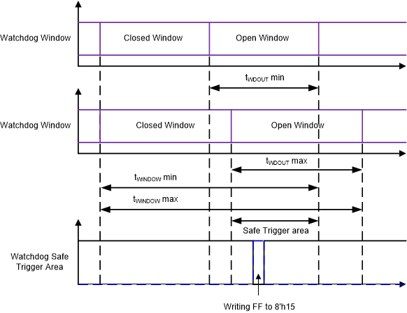
When using the window watchdog it is important to understand the closed and open window aspects. The device is set up with a 50%/50% open and closed window and is based on an internal oscillator with a ± 10% accuracy range. To determine when to provide the input trigger, this variance needs to be taken into account. Using the 60 ms nominal total window provides a closed and open window that are each 30 ms. Taking the ± 10% internal oscillator into account means the total window could be 54 ms, tWINDOW, MIN or 66 ms, tWINDOW MAX. The closed and open window would then be 27 ms, TWDOUT MIN, or 33 ms, TWDOUT MIN. From the 54 ms total window and 33 ms closed window the total open window is 21 ms. The trigger event needs to happen at the 43.5 ms ± 10.5 ms, safe trigger area. The same method is used for the other window values. Figure 9-4 provides the above information graphically. Once the WD trigger is written, the current Window is terminated and a new Closed Window is started.
 Figure 9-4 Window Watchdog Timing Diagram