ZHCSPC3A May   2021  – November 2021 TCAN11623-Q1 , TCAN11625-Q1

PRODUCTION DATA  

  1. 特性
  2. 应用
  3. 说明
  4. Revision History
  5. 说明(续)
  6. Pin Configurations and Functions (TCAN11625)
  7. Pin Configurations and Functions (TCAN11623)
  8. Specifications
    1. 8.1 Absolute Maximum Ratings
    2. 8.2 ESD Ratings
    3. 8.3 ESD Ratings IEC Specification
    4. 8.4 Recomended Operating Conditions
    5. 8.5 Thermal Information
    6. 8.6 Power Supply Characteristics
    7. 8.7 Electrical Characteristics
    8. 8.8 Switching Characteristics
    9. 8.9 Typical Characteristics
  9. Parameter Measurement Information
  10. 10Detailed Description
    1. 10.1 Overview
    2. 10.2 Functional Block Diagram
    3. 10.3 Feature Description
      1. 10.3.1  VSUP Pin
      2. 10.3.2  VCCOUT Pin
      3. 10.3.3  VFLT Pin
      4. 10.3.4  VLDO3 Pin
      5. 10.3.5  Digital Inputs and Outputs
        1. 10.3.5.1 TXD Pin
        2. 10.3.5.2 RXD Pin
        3. 10.3.5.3 TS Pin
      6. 10.3.6  Digital Control and Timing
      7. 10.3.7  VIO Pin
      8. 10.3.8  GND
      9. 10.3.9  INH Pin
      10. 10.3.10 WAKE Pin
      11. 10.3.11 nRST Pin
      12. 10.3.12 CAN Bus Pins
      13. 10.3.13 Local Faults
        1. 10.3.13.1 TXD Dominant Timeout (TXD DTO)
        2. 10.3.13.2 Thermal Shutdown (TSD)
        3. 10.3.13.3 Under/Over Voltage Lockout
        4. 10.3.13.4 Unpowered Devices
        5. 10.3.13.5 Floating Terminals
        6. 10.3.13.6 CAN Bus Short Circuit Current Limiting
        7. 10.3.13.7 Sleep Wake Error Timer
    4. 10.4 Device Functional Modes
      1. 10.4.1 Operating Mode Description
        1. 10.4.1.1 Normal Mode
        2. 10.4.1.2 Standby Mode
        3. 10.4.1.3 Sleep Mode
          1. 10.4.1.3.1 Remote Wake Request via Wake-Up Pattern (WUP)
          2. 10.4.1.3.2 Local Wake-Up (LWU) via WAKE Input Terminal
        4. 10.4.1.4 Reset Mode
        5. 10.4.1.5 Fail-safe Mode
      2. 10.4.2 CAN Transceiver
        1. 10.4.2.1 CAN Transceiver Operation
        2. 10.4.2.2 CAN Transceiver Modes
          1. 10.4.2.2.1 CAN Off Mode
          2. 10.4.2.2.2 CAN Autonomous: Inactive and Active
          3. 10.4.2.2.3 CAN Active
        3. 10.4.2.3 Driver and Receiver Function Tables
        4. 10.4.2.4 CAN Bus States
  11. 11Application Information
    1. 11.1 Application Information Disclaimer
    2. 11.2 Typical Application
      1. 11.2.1 Design Requirements
        1. 11.2.1.1 Bus Loading, Length and Number of Nodes
      2. 11.2.2 Detailed Design Procedures
        1. 11.2.2.1 CAN Termination
    3. 11.3 Application Curves
  12. 12Power Supply Requirements
  13. 13Layout
    1. 13.1 Layout Guidelines
    2. 13.2 Layout Example
  14. 14Device and Documentation Support
    1. 14.1 Documentation Support
      1. 14.1.1 Related Documentation
    2. 14.2 接收文档更新通知
    3. 14.3 支持资源
    4. 14.4 Trademarks
    5. 14.5 Electrostatic Discharge Caution
    6. 14.6 术语表
  15. 15Mechanical, Packaging, and Orderable Information

封装选项

机械数据 (封装 | 引脚)
散热焊盘机械数据 (封装 | 引脚)
订购信息

Pin Configurations and Functions (TCAN11625)

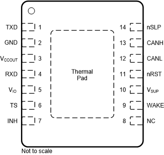
GUID-0A447BD0-72BC-49F8-B0B4-CD440C211CCA-low.gif Figure 6-1 DMT Package, 14 Pin (VSON), Top View
Table 6-1 Pin Functions
PINSTYPEDESCRIPTION
NAMENO.
TXD1DigitalCAN transmit data input, integrated pull-up
GND2GNDGround connection
VCCOUT3Supply5-V LDO regulated output voltage pin and transceiver supply
RXD4DigitalCAN receive data output, tri-state when VIO < UVVIO
VIO5SupplyIO supply voltage
TS6DigitalTransceiver status
INH7High VoltageInhibit pin to control system voltage regulators and supplies, high voltage
NC8Internally connected, leave floating or connect to GND
WAKE9High VoltageLocal WAKE input terminal, high voltage
VSUP10SupplyHigh voltage supply from the battery
nRST11DigitalReset input/output
CANL12Bus IOLow level CAN bus input/output line
CANH13Bus IOHigh level CAN bus input/output line
nSLP14DigitalSleep mode control input, integrated pull-down
Thermal PadElectrically connected to GND, connect the thermal pad to the printed circuit board (PCB) ground plane for thermal relief