SCAS339S March 1994 – February 2017 SN74LVC126A
PRODUCTION DATA.
- 1 Features
- 2 Applications
- 3 Description
- 4 Revision History
- 5 Pin Configuration and Functions
- 6 Specifications
- 7 Parameter Measurement Information
- 8 Detailed Description
- 9 Application and Implementation
- 10Power Supply Recommendations
- 11Layout
- 12Device and Documentation Support
- 13Mechanical, Packaging, and Orderable Information
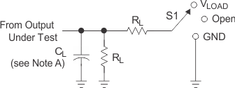
7 Parameter Measurement Information
 Figure 2. Load Circuit
Table 1. Timing Test Conditions
| TEST | S1 |
|---|---|
| tPLH and tPHL | Open |
| tPLZ and tPZL | VLOAD |
| tPHZ and tPZH | GND |
Table 2. Electrical Characteristics Test Conditions
| VCC | INPUTS | VM | VLOAD | CL | RL | VΔ | |
|---|---|---|---|---|---|---|---|
| VI | tr/tf | ||||||
| 1.8 V ± 0.15 V | VCC | ≤2 ns | VCC/2 | 2 × VCC | 30 pF | 1 kΩ | 0.15 V |
| 2.5 V ± 0.2 V | VCC | ≤2 ns | VCC/2 | 2 × VCC | 30 pF | 500 Ω | 0.15 V |
| 2.7 V | 2.7 V | ≤2.5 ns | 1.5 V | 6 V | 50 pF | 500 Ω | 0.3 V |
| 3.3 V ± 0.3 V | 2.7 V | ≤2.5 ns | 1.5 V | 6 V | 50 pF | 500 Ω | 0.3 V |
 Figure 3. Voltage Waveforms,
Pulse Duration
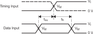
 Figure 4. Voltage Waveforms,
Setup and Hold Times
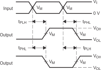
 Figure 5. Voltage Waveforms, Propagation Delay Times Inverting and Noninverting Outputs

A. CL includes probe and jig capacitance.
B. Waveform 1 is for an output with internal conditions such that the output is low, except when disables by the output control. Waveform 2 is for an output with internal conditions such that the output is high, except when disabled by the output control.
C. All input pulses are supplied by generators having the following characteristics: PRR ≤ 10 MHz, ZO = 50 Ω.
D. The outputs are measured one at a time, with one transition per measurement.
E. tPLZ and tPHZ are the same as tdis.
F. tPZL and tPZH are the same as ten.
G. tPLH and tPHL are the same as tpd.
H. All parameters and waveforms are not applicable to all devices.
Figure 6. Voltage Waveforms, Enable and Disable Times Low- and High-Level Enabling