ZHCS601D December 2011 – May 2015 SN65HVD255 , SN65HVD256 , SN65HVD257
PRODUCTION DATA.
- 1 特性
- 2 应用
- 3 说明
- 4 修订历史记录
- 5 Device Options
- 6 Pin Configuration and Functions
- 7 Specifications
- 8 Parameter Measurement Information
- 9 Detailed Description
- 10Application and Implementation
- 11Power Supply Recommendations
- 12Layout
- 13器件和文档支持
- 14机械、封装和可订购信息
8 Parameter Measurement Information
 Figure 6. Driver Test Circuit and Measurement
 Figure 7. Receiver Test Circuit and Measurement
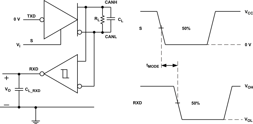
 Figure 8. tMODE Test Circuit and Measurement
Table 1. Receiver Differential Input Voltage Threshold Test
| INPUT | OUTPUT | |||
|---|---|---|---|---|
| VCANH | VCANL | |VID| | RXD | |
| –1.1 V | –2.0 V | 900 mV | L | VOL |
| 7.0 V | 6.1 V | 900 mV | L | |
| –1.5 V | –2.0 V | 500 mV | H | VOH |
| 7.0 V | 6.5 V | 500 mV | H | |
| Open | Open | X | H | |
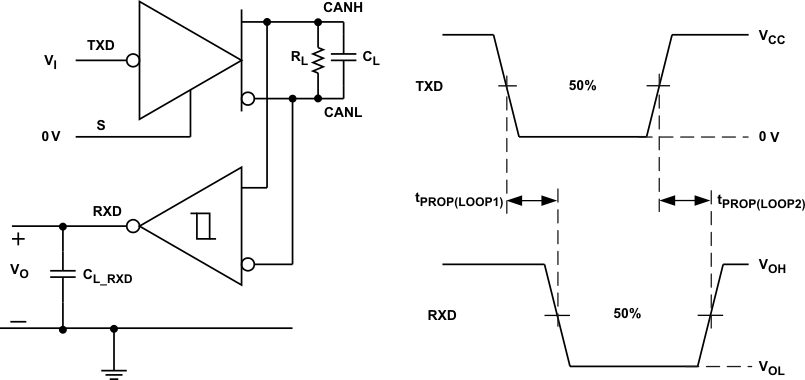
 Figure 9. TPROP(LOOP) Test Circuit and Measurement
 Figure 10. TXD Dominant Timeout Test Circuit and Measurement
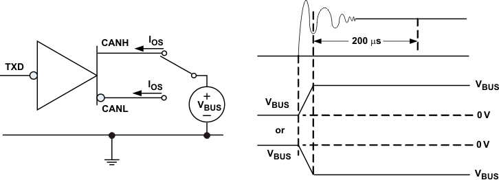
 Figure 11. Driver Short Circuit Current Test and Measurement

