SGUS033A February 2002 – May 2016 SMJ320C6203
PRODUCTION DATA.
- 1 Features
- 2 Description
- 3 Revision History
- 4 Description (continued)
- 5 Characteristics of the C6203 DSP
- 6 Pin Configuration and Functions
-
7 Specifications
- 7.1 Absolute Maximum Ratings
- 7.2 Recommended Operating Conditions
- 7.3 Thermal Information
- 7.4 Electrical Characteristics
- 7.5 Timing Requirements for CLKIN (PLL Used)
- 7.6 Timing Requirements for CLKIN [PLL Bypassed (x1)]
- 7.7 Timing Requirements for XCLKIN
- 7.8 Timing Requirements for Asynchronous Memory Cycles
- 7.9 Timing Requirements for Synchronous-Burst SRAM Cycles
- 7.10 Timing Requirements for Synchronous DRAM Cycles
- 7.11 Timing Requirements for the HOLD/HOLDA Cycles
- 7.12 Timing Requirements for Reset
- 7.13 Timing Requirements for Interrupt Response Cycles
- 7.14 Timing Requirements for Synchronous FIFO Interface
- 7.15 Timing Requirements for Asynchronous Peripheral Cycles
- 7.16 Timing Requirements With External Device as Bus Master
- 7.17 Timing Requirements With C62x as Bus Master
- 7.18 Timing Requirements With External Device as Asynchronous Bus Master
- 7.19 Timing Requirements for Expansion Bus Arbitration (Internal Arbiter Enabled)
- 7.20 Timing Requirements for McBSP
- 7.21 Timing Requirements for FSR when GSYNC = 1
- 7.22 Timing Requirements for McBSP as SPI Master or Slave: CLKSTP = 10b, CLKXP = 0
- 7.23 Timing Requirements for McBSP as SPI Master or Slave: CLKSTP = 11b, CLKXP = 0
- 7.24 Timing Requirements for McBSP as SPI Master or Slave: CLKSTP = 10b, CLKXP = 1
- 7.25 Timing Requirements for McBSP as SPI Master or Slave: CLKSTP = 11b, CLKXP = 1
- 7.26 Timing Requirements for Timer Inputs
- 7.27 Timing Requirements for JTAG Test Port
- 7.28 Switching Characteristics for CLKOUT2
- 7.29 Switching Characteristics for XFCLK
- 7.30 Asynchronous Memory Timing Switching Characteristics
- 7.31 Switching Characteristics for Synchronous-Burst SRAM Cycles
- 7.32 Switching Characteristics for Synchronous DRAM Cycles
- 7.33 Switching Characteristics for the HOLD/HOLDA Cycles
- 7.34 Switching Characteristics for Reset
- 7.35 Switching Characteristics for Interrupt Response Cycles
- 7.36 Switching Characteristics for Synchronous FIFO Interface
- 7.37 Switching Characteristics for Asynchronous Peripheral Cycles
- 7.38 Switching Characteristics With External Device as Bus Master
- 7.39 Switching Characteristics With C62x as Bus Master
- 7.40 Switching Characteristics With External Device as Asynchronous Bus Master
- 7.41 Switching Characteristics for Expansion Bus Arbitration (Internal Arbiter Enabled)
- 7.42 Switching Characteristics for Expansion Bus Arbitration (Internal Arbiter Disabled)
- 7.43 Switching Characteristics for McBSP
- 7.44 Switching Characteristics for McBSP as SPI Master or Slave
- 7.45 Switching Characteristics for McBSP as SPI Master or Slave: CLKSTP = 11b, CLKXP = 0
- 7.46 Switching Characteristics for McBSP as SPI Master or Slave: CLKSTP = 10b, CLKXP = 1
- 7.47 Switching Characteristics for McBSP as SPI Master or Slave: CLKSTP = 11b, CLKXP = 1
- 7.48 Switching Characteristics for DMAC Outputs
- 7.49 Switching Characteristics for Timer Outputs
- 7.50 Switching Characteristics for Power-Down Outputs
- 7.51 Switching Characteristics for JTAG Test Port
- 8 Parameter Measurement Information
- 9 Detailed Description
- 10Application and Implementation
- 11Power Supply Recommendations
- 12Device and Documentation Support
- 13Mechanical, Packaging, and Orderable Information
8 Parameter Measurement Information
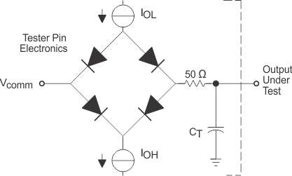
8.1 Signal Transition Levels
All input and output timing parameters are referenced to 1.5 V for both 0 and 1 logic levels.
 Figure 2. Input and Output Voltage Reference Levels for AC Timing Measurements
All rise and fall transition timing parameters are referenced to VIL MAX and VIH MIN for input clocks, and VOL MAX and VOH MIN for output clocks.
 Figure 3. Rise and Fall Transition Time Voltage Reference Levels
8.2 Timing Parameters and Board Routing Analysis
The timing parameter values specified in this data sheet do not include delays by board routings. As a good board design practice, always account for such delays. Timing values may be adjusted by increasing/decreasing such delays. TI recommends using the available I/O buffer information specification (IBIS) models to analyze the timing characteristics correctly. If needed, external logic hardware such as buffers may be used to compensate any timing differences.
For inputs, timing is most impacted by the round-trip propagation delay from the DSP to the external device and from the external device to the DSP. This round-trip delay tends to negatively impact the input setup time margin, but also tends to improve the input hold time margins (see Table 1 and Figure 4).
Figure 4 represents a general transfer between the DSP and an external device. Figure 4 also represents board route delays and how they are perceived by the DSP and the external device.
Table 1. IBIS Timing Parameters Example (See Figure 4)
| NO. | DESCRIPTION |
|---|---|
| 1 | Clock route delay |
| 2 | Minimum DSP hold time |
| 3 | Minimum DSP setup time |
| 4 | External device hold time requirement |
| 5 | External device setup time requirement |
| 6 | Control signal route delay |
| 7 | External device hold time |
| 8 | External device access time |
| 9 | DSP hold time requirement |
| 10 | DSP setup time requirement |
| 11 | Data route delay |
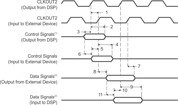
- Control signals include data for Writes.
- Data signals are generated during Reads from an external device.
 Figure 5. CLKIN Timings
 Figure 6. XCLKIN Timings
 Figure 7. CLKOUT2 Timings
 Figure 8. XFCLK Timings
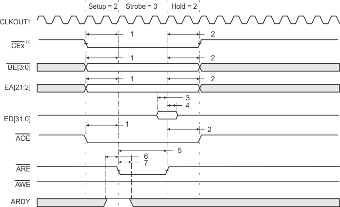
- CEx stays active for 7 – the value of Read Hold cycles after the last access (DMA transfer or CPU access). For example, if read HOLD = 1, then CEx stays active for six more cycles. This does not affect performance, it merely reflects the overhead of the EMIF.
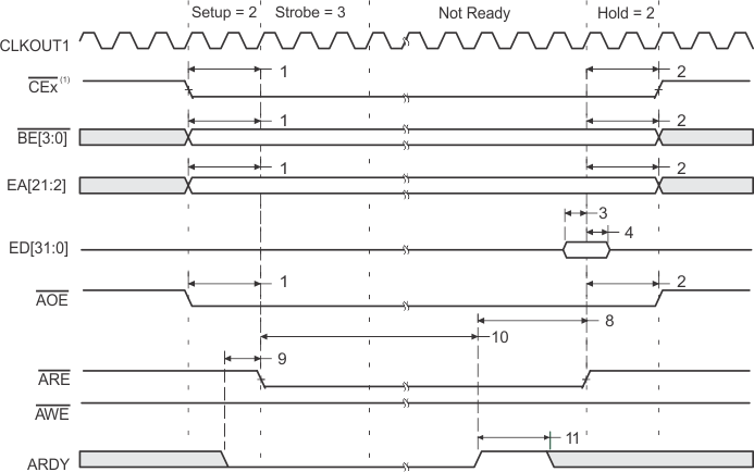
- CEx stays active for 7 – the value of Read Hold cycles after the last access (DMA transfer or CPU access). For example, if read HOLD = 1, then CEx stays active for six more cycles. This does not affect performance, it merely reflects the overhead of the EMIF.
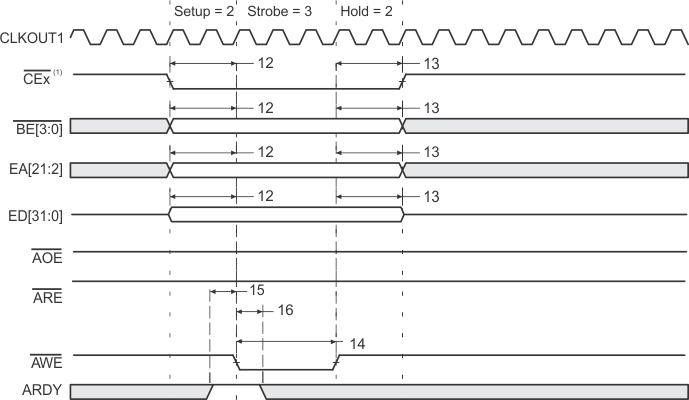
- If no write accesses are scheduled for the next cycle and write hold is set to 1 or greater, then CEx stays active for three cycles after the value of the programmed hold period. If write hold is set to 0, then CEx stays active for four more cycles. This does not affect performance, it merely reflects the overhead of the EMIF.
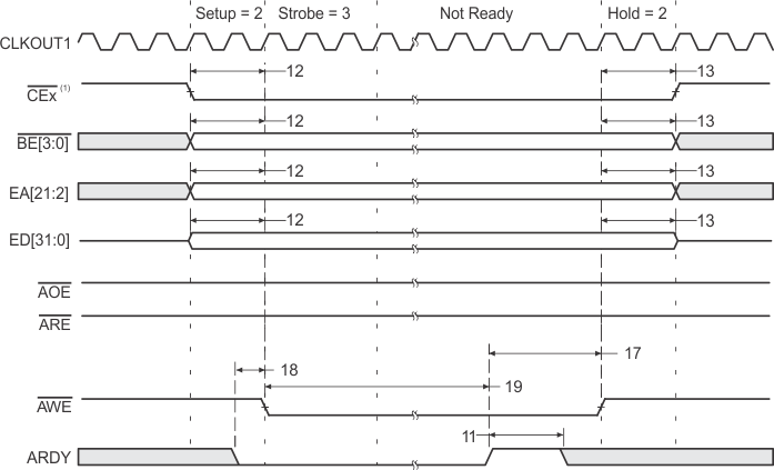
- If no write accesses are scheduled for the next cycle and write hold is set to 1 or greater, then CEx stays active for three cycles after the value of the programmed hold period. If write hold is set to 0, then CEx stays active for four more cycles. This does not affect performance, it merely reflects the overhead of the EMIF.
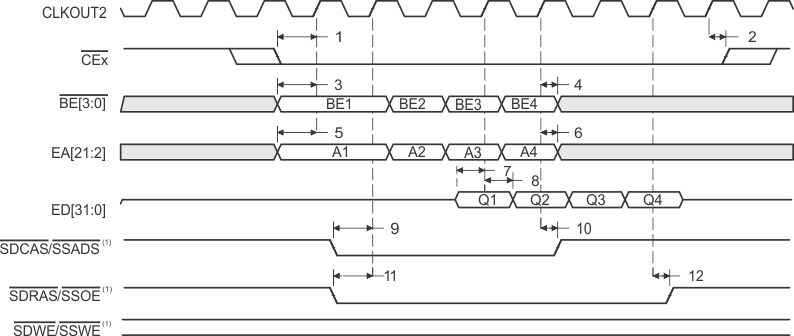
- SDCAS/SSADS, SDRAS/SSOE, and SDWE/SSWE operate as SSADS, SSOE, and SSWE, respectively, during SBSRAM accesses.
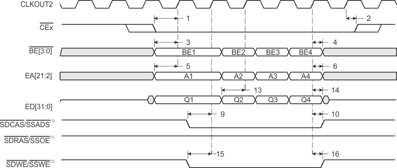
- SDCAS/SSADS, SDRAS/SSOE, and SDWE/SSWE operate as SSADS, SSOE, and SSWE, respectively, during SBSRAM accesses.
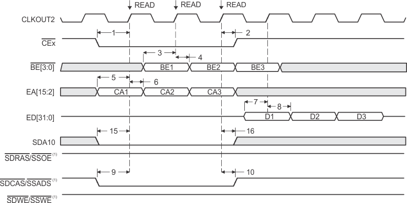
- SDCAS/SSADS, SDRAS/SSOE, and SDWE/SSWE operate as SDCAS, SDRAS, and SDWE, respectively, during SDRAM accesses.
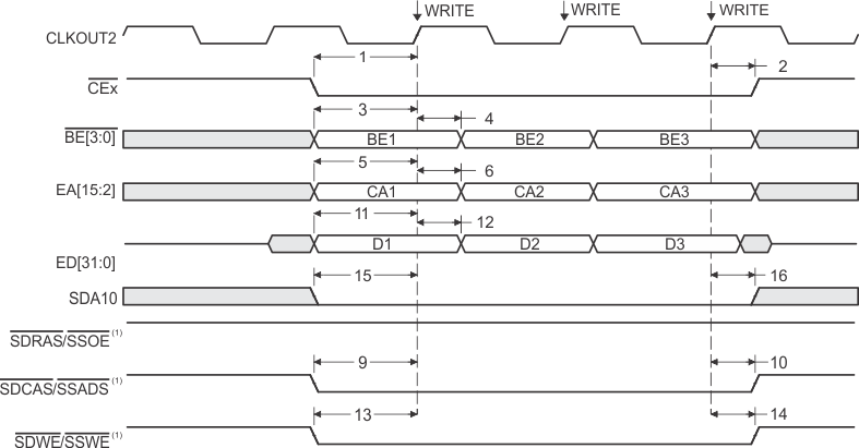
- SDCAS/SSADS, SDRAS/SSOE, and SDWE/SSWE operate as SDCAS, SDRAS, and SDWE, respectively, during SDRAM accesses.
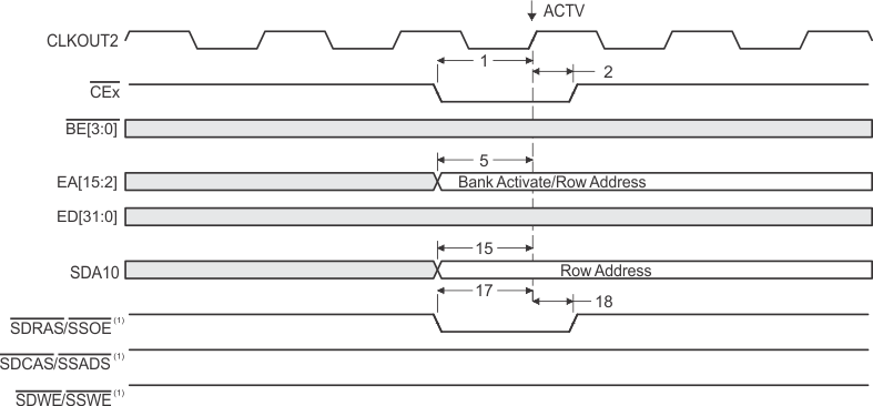
- SDCAS/SSADS, SDRAS/SSOE, and SDWE/SSWE operate as SDCAS, SDRAS, and SDWE, respectively, during SDRAM accesses.
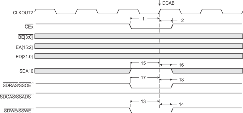
- SDCAS/SSADS, SDRAS/SSOE, and SDWE/SSWE operate as SDCAS, SDRAS, and SDWE, respectively, during SDRAM accesses.
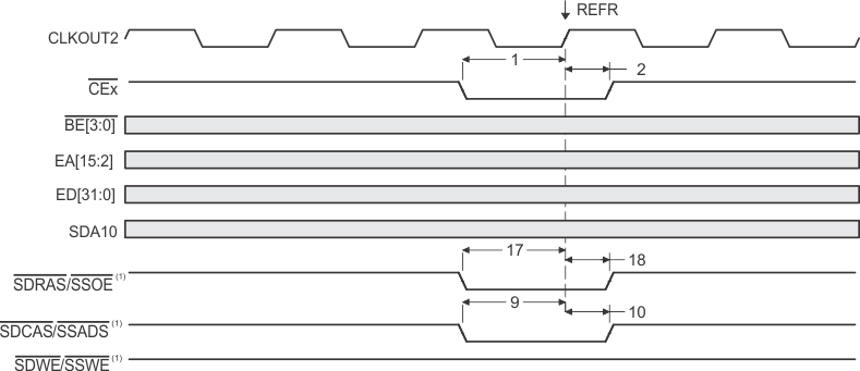
- SDCAS/SSADS, SDRAS/SSOE, and SDWE/SSWE operate as SDCAS, SDRAS, and SDWE, respectively, during SDRAM accesses.
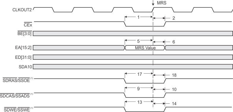
- SDCAS/SSADS, SDRAS/SSOE, and SDWE/SSWE operate as SDCAS, SDRAS, and SDWE, respectively, during SDRAM accesses.

- EMIF bus consists of CE[3:0], BE[3:0], ED[31:0], EA[21:2], ARE, AOE, AWE, SDCAS/SSADS, SDRAS/SSOE, SDWE/SSWE, and SDA10.
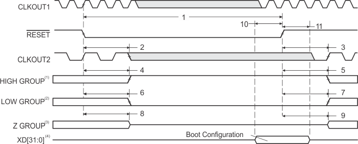
- High group consists of: XFCLK, HOLDA
- Low group consists of: IACK, INUM[3:0], DMAC[3:0], PD, TOUT0, and TOUT1
- Z group consists of: EA[21:2], ED[31:0], CE[3:0], BE[3:0], ARE, AWE, AOE, SDCAS/SSADS, SDRAS/SSOE, SDWE/SSWE, SDA10, CLKX0, CLKX1, CLKX2, FSX0, FSX1, FSX2, DX0, DX1, DX2, CLKR0, CLKR1, CLKR2, FSR0, FSR1, FSR2, XCE[3:0], XBE[3:0]/XA[5:2], XOE, XRE, XWE/XWAIT, XAS, XW/R, XRDY, XBLAST, XHOLD, and XHOLDA
- XD[31:0] are the boot configuration pins during device reset.
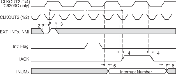 Figure 23. Interrupt Timing
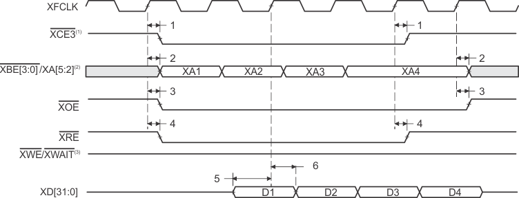
- FIFO read (glueless) mode only available in XCE3.
- XBE[3:0]/XA[5:2] operate as address signals XA[5:2] during synchronous FIFO accesses.
- XWE/XWAIT operate as the write-enable signal XWE during synchronous FIFO accesses.
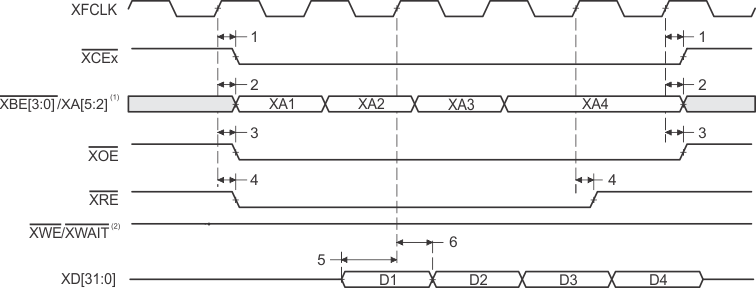
- XBE[3:0]/XA[5:2] operate as address signals XA[5:2] during synchronous FIFO accesses.
- XWE/XWAIT operate as the write-enable signal XWE during synchronous FIFO accesses.
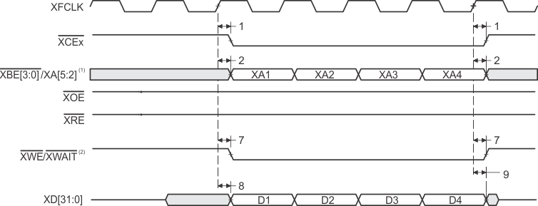
- XBE[3:0]/XA[5:2] operate as address signals XA[5:2] during synchronous FIFO accesses.
- XWE/XWAIT operate as the write-enable signal XWE during synchronous FIFO accesses.
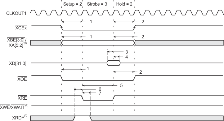
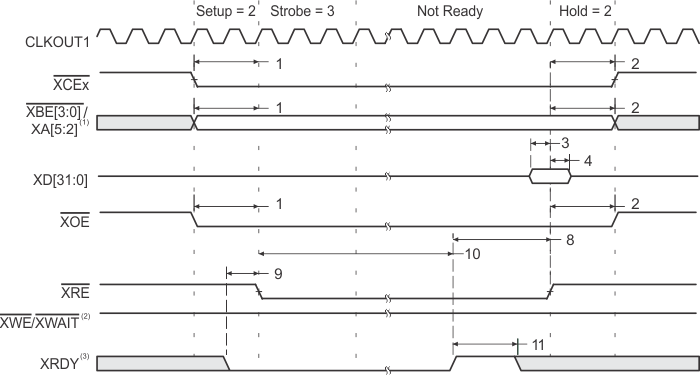
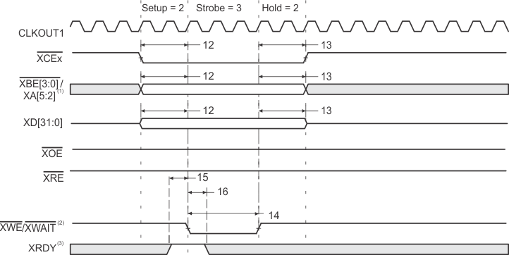
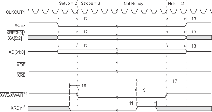
- XBE[3:0]/XA[5:2] operate as address signals XA[5:2] during expansion bus asynchronous peripheral accesses.
- XWE/XWAIT operate as the write-enable signal XWE during expansion bus asynchronous peripheral accesses.
- XRDY operates as active-high ready input during expansion bus asynchronous peripheral accesses.
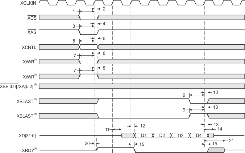
- XW/R input/output polarity selected at boot
- XBE[3:0]/XA[5:2] operate as byte-enables XBE[3:0] during host-port accesses.
- XBLAST input polarity selected at boot
- XRDY operates as active-low ready input/output during host-port accesses.
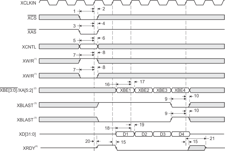
- XW/R input/output polarity selected at boot
- XBE[3:0]/XA[5:2] operate as byte-enables XBE[3:0] during host-port accesses.
- XBLAST input polarity selected at boot
- XRDY operates as active-low ready input/output during host-port accesses.
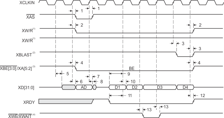
- XW/R input/output polarity selected at boot
- XBLAST output polarity is always active low.
- XBE[3:0]/XA[5:2] operate as byte-enables XBE[3:0] during host-port accesses.
- XWE/XWAIT operate as XWAIT output signal during host-port accesses.
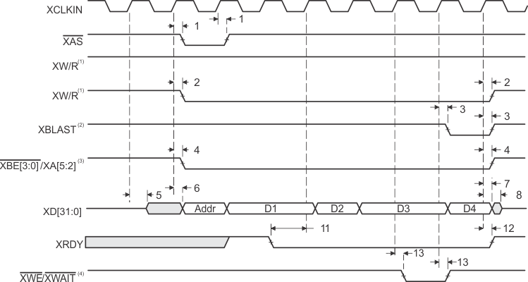
- XW/R input/output polarity selected at boot
- XBLAST output polarity is always active low.
- XBE[3:0]/XA[5:2] operate as byte-enables XBE[3:0] during host-port accesses.
- XWE/XWAIT operate as XWAIT output signal during host-port accesses.
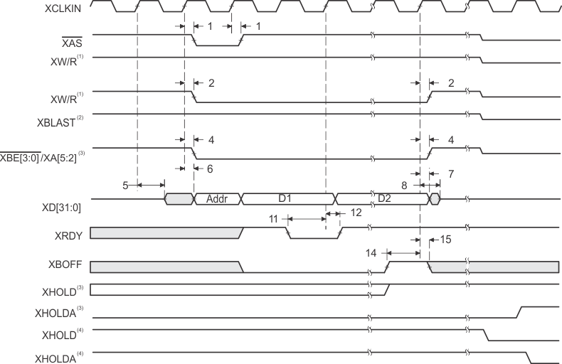
- XW/R input/output polarity selected at boot
- XBLAST output polarity is always active low.
- XBE[3:0]/XA[5:2] operate as byte-enables XBE[3:0] during host-port accesses.
- Internal arbiter enabled
- External arbiter enabled
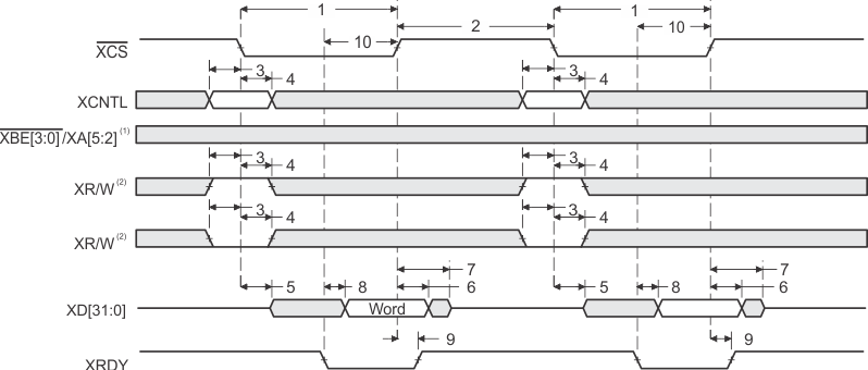
- XBE[3:0]/XA[5:2] operate as byte-enables XBE[3:0] during host-port accesses.
- XW/R input/output polarity selected at boot
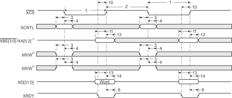
- XBE[3:0]/XA[5:2] operate as byte-enables XBE[3:0] during host-port accesses.
- XW/R input/output polarity selected at boot

- Expansion bus consists of XBE[3:0]/XA[5:2], XAS, XW/R, and XBLAST.

- Expansion bus consists of XBE[3:0]/XA[5:2], XAS, XW/R, and XBLAST.
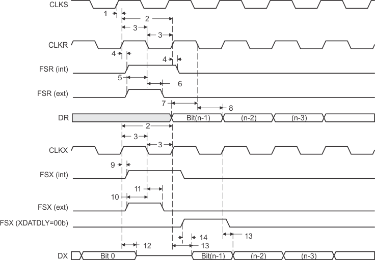 Figure 40. McBSP Timings
 Figure 41. FSR Timing When GSYNC = 1
 Figure 42. McBSP Timing as SPI Master or Slave: CLKSTP = 10b, CLKXP = 0
 Figure 43. McBSP Timing as SPI Master or Slave: CLKSTP = 11b, CLKXP = 0
 Figure 44. McBSP Timing as SPI Master or Slave: CLKSTP = 10b, CLKXP = 1
 Figure 45. McBSP Timing as SPI Master or Slave: CLKSTP = 11b, CLKXP = 1
 Figure 46. DMAC Timing
 Figure 47. Timer Timing
 Figure 48. Power-Down Timing
 Figure 49. JTAG Test-Port Timing