SLFS022I September 1973 – September 2014 NA555 , NE555 , SA555 , SE555
PRODUCTION DATA.
- 1 Features
- 2 Applications
- 3 Description
- 4 Simplified Schematic
- 5 Revision History
- 6 Pin Configuration and Functions
- 7 Specifications
- 8 Detailed Description
- 9 Applications and Implementation
- 10Power Supply Recommendations
- 11Device and Documentation Support
- 12Mechanical, Packaging, and Orderable Information
1 Features
- Timing From Microseconds to Hours
- Astable or Monostable Operation
- Adjustable Duty Cycle
- TTL-Compatible Output Can Sink or Source
Up to 200 mA -
On Products Compliant to MIL-PRF-38535,
All Parameters Are Tested Unless Otherwise Noted. On All Other Products, Production Processing Does Not Necessarily Include
Testing of All Parameters.
3 Description
These devices are precision timing circuits capable of producing accurate time delays or oscillation. In the time-delay or mono-stable mode of operation, the timed interval is controlled by a single external resistor and capacitor network. In the a-stable mode of operation, the frequency and duty cycle can be controlled independently with two external resistors and a single external capacitor.
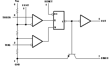
The threshold and trigger levels normally are two-thirds and one-third, respectively, of VCC. These levels can be altered by use of the control-voltage terminal. When the trigger input falls below the trigger level, the flip-flop is set, and the output goes high. If the trigger input is above the trigger level and the threshold input is above the threshold level, the flip-flop is reset and the output is low. The reset (RESET) input can override all other inputs and can be used to initiate a new timing cycle. When RESET goes low, the flip-flop is reset, and the output goes low. When the output is low, a low-impedance path is provided between discharge (DISCH) and ground.
The output circuit is capable of sinking or sourcing current up to 200 mA. Operation is specified for supplies of 5 V to 15 V. With a 5-V supply, output levels are compatible with TTL inputs.
Device Information(1)
| PART NUMBER | PACKAGE | BODY SIZE (NOM) |
|---|---|---|
| xx555 | PDIP (8) | 9.81 mm × 6.35 mm |
| SOP (8) | 6.20 mm × 5.30 mm | |
| TSSOP (8) | 3.00 mm × 4.40 mm | |
| SOIC (8) | 4.90 mm × 3.91 mm |
- For all available packages, see the orderable addendum at the end of the datasheet.
4 Simplified Schematic
