SBAS452A September 2008 – January 2016 PCM3168A
PRODUCTION DATA.
- 1 Features
- 2 Applications
- 3 Description
- 4 Revision History
- 5 Description (continued)
- 6 Device Comparison Table
- 7 Pin Configuration and Functions
-
8 Specifications
- 8.1 Absolute Maximum Ratings
- 8.2 ESD Ratings
- 8.3 Recommended Operating Conditions
- 8.4 Thermal Information
- 8.5 Electrical Characteristics
- 8.6 Timing Requirements: System Clock
- 8.7 Timing Requirements: Power-On Reset
- 8.8 Timing Requirements: Audio Interface for Left-Justified, Right-Justified, and I2S (Slave Mode)
- 8.9 Timing Requirements: Audio Interface for Left-Justified, Right-Justified, and I2S (Master Mode)
- 8.10 Timing Requirements: Audio Interface for DSP and TDM (Slave Mode)
- 8.11 Timing Requirements: Audio Interface for DSP and TDM (Master Mode)
- 8.12 Timing Requirements: DAC Outputs and ADC Outputs
- 8.13 Timing Requirements: Four-Wire Serial Control Interface
- 8.14 Timing Requirements: SCL and SDA Control Interface
- 8.15 Typical Characteristics
-
9 Detailed Description
- 9.1 Overview
- 9.2 Functional Block Diagram
- 9.3
Feature Description
- 9.3.1 Analog Inputs
- 9.3.2 Analog Outputs
- 9.3.3 Voltage References
- 9.3.4 System Clock Input
- 9.3.5 Sampling Mode
- 9.3.6 Reset Operation
- 9.3.7 Highpass Filter (HPF)
- 9.3.8 Overflow Flag
- 9.3.9 Zero Flag
- 9.3.10 Four-Wire (SPI) Serial Control
- 9.3.11 Control Data Word Format
- 9.3.12 Register Write Operation
- 9.3.13 Register Read Operation
- 9.3.14 Two-Wire (I2C) Serial Control
- 9.3.15 Packet Protocol
- 9.3.16 Write Operation
- 9.3.17 Read Operation
- 9.4 Device Functional Modes
- 9.5 Register Maps
- 10Application and Implementation
- 11Power Supply Recommendations
-
12Layout
- 12.1
Layout Guidelines
- 12.1.1 Power-Supply Pins (VCCAD1/2, VCCDA1/2, and VDD1/2)
- 12.1.2 Grounding (AGNDAD1/2, AGNDDA1/2, and DGND1/2)
- 12.1.3 VIN1±, VIN2±, VIN3±, VIN4±, VIN5±, and VIN6± Pins
- 12.1.4 VCOMAD and VCOMDA Pins
- 12.1.5 VREFAD1/2 Pins
- 12.1.6 VOUT1±, VOU2±, VOUT3±, VOUT4±, VOUT5±, VOUT6±, VOUT7±, and VOUT8± Pins
- 12.1.7 MODE Pin
- 12.1.8 RST Pin
- 12.1.9 OVF Pin
- 12.1.10 System Clock and Audio Interface Clocks
- 12.1.11 PowerPAD
- 12.1.12 External Mute Control
- 12.2 Layout Example
- 12.1
Layout Guidelines
- 13Device and Documentation Support
- 14Mechanical, Packaging, and Orderable Information
10 Application and Implementation
NOTE
Information in the following applications sections is not part of the TI component specification, and TI does not warrant its accuracy or completeness. TI’s customers are responsible for determining suitability of components for their purposes. Customers should validate and test their design implementation to confirm system functionality.
10.1 Application Information
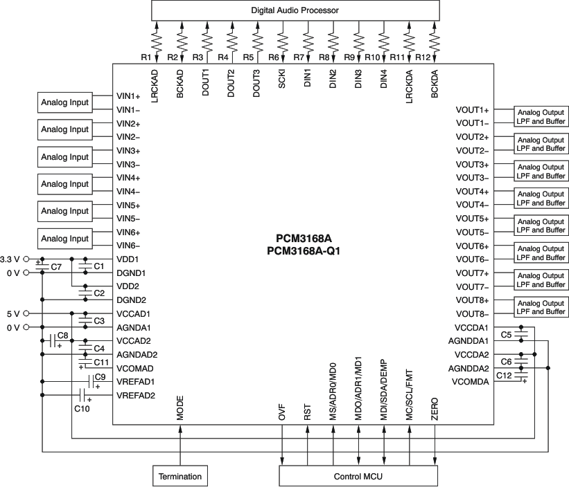
A typical circuit connection for six-channel analog in and eight-channel analog out is shown in Figure 54.
10.2 Typical Application
NOINDENT:
C1 through C6 are 1-μF ceramic capacitors dependent on power-supply quality. C7 and C8 are 10-μF electrolytic capacitors dependent on power-supply quality. C9 and C10 are 10-μF electrolytic capacitors. C11 and C12 are 10-μF electrolytic capacitors. R1 through R12 are 22-Ω to 100-Ω resistors.10.2.1 Design Requirements
For this design example, use the parameters listed in Table 14.
Table 14. Design Parameters
| DESIGN PARAMETER | EXAMPLE VALUE |
|---|---|
| Audio input | PCM audio, differential analog audio |
| Audio output | PCM audio, differential analog audio |
| Control | I2C, SPI |
10.2.2 Detailed Design Procedure
10.2.2.1 Analog Input and Output
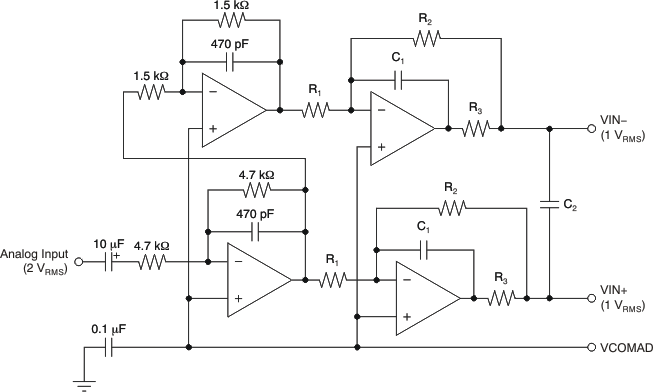
It is recommended that input and output filters be used to condition the inputs and outputs. Input filters can be used to convert a single ended signal into a differential signal while also attenuating out of band noise. Another use of an input filter for the ADC it to reduce a 2-VRMS signal to a 1-VRMS input, which is the limit of the ADC input. Output filters can be used to go from differential to single ended, while reducing a differential signal that is 8 VPP to a 2-VRMS signal. The output filter can also attenuate out of band noise.
10.2.2.2 PCM Interface
The PCM3168A has the capability of inputting 8 PCM channels over 4 data pins in normal PCM mode, or can operate in TDM mode to take in 8 channels on one data pin. The PCM3168A can also output up to 6 PCM channels over 3 data pins, or over 1 pin in TDM mode.
10.2.3 Application Curves
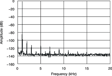
| –1 dB, N = 32768 | ||
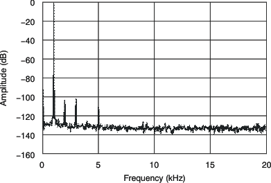
| 0 dB, N = 32768 | ||
10.3 System Examples
10.3.1 Typical Circuit Connections
Termination for mode control: Any one of the circuits shown in Figure 57 must be applied according to the necessary mode or configuration. Resistor value must be 220-kΩ, ±5% tolerant. The PowerPAD must be tied to the ground plane with enough electrical and thermal conductivity; see the example board layout in Figure 54.
 Figure 57. Typical Circuit Connections
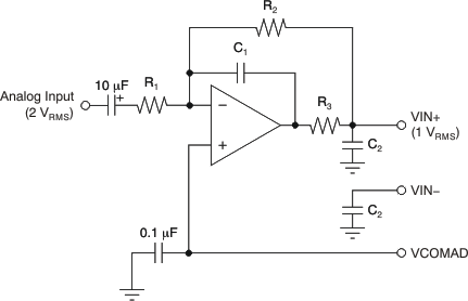
Typical interface circuits for analog input and analog output are shown in Figure 58 through Figure 62.
NOINDENT:
NOINDENT:
Amplifier is an NE5532A x1 or OPA2134 x1; R1 = 3-kΩ resistor; R2 = 1.5-kΩ resistor; R3 = 47-Ω resistor; C1 = 2200-pF capacitor; C2 = 0.022-μF capacitor; Gain = 0.5; f–3 dB = 48 kHz.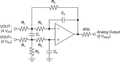
NOINDENT:
Amplifier is an NE5532A x1/2 or OPA2134 x1/2; R1 = 15-kΩ resistor; R2 = 11-kΩ resistor; R3 = 820-Ω resistor; C1 = 1500-pF capacitor; C2 = 330-pF capacitor; Gain = 0.733; f–3 dB = 54 kHz.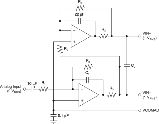
NOINDENT:
Amplifier is an NE5532A x1 or OPA2134 x1; R1 = 3-kΩ resistor; R2 = 1.5-kΩ resistor; R3 = 47-Ω resistor; C1 = 2200-pF capacitor; C2 = 0.01-μF capacitor; Gain = 1; f–3 dB = 48 kHz.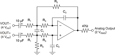
NOINDENT:
 Figure 63. Basic Differential Input Circuit With Anti-Aliasing LPF for Differential ADC Input