ZHCSG67A March   2017  – December 2018 OPT3001-Q1

PRODUCTION DATA.  

  1. 特性
  2. 应用
  3. 说明
    1.     框图
    2.     光谱响应:OPT3001-Q1 和人眼
  4. 修订历史记录
  5. 说明 (续)
  6. Pin Configuration and Functions
    1.     Pin Functions
  7. Specifications
    1. 7.1 Absolute Maximum Ratings
    2. 7.2 ESD Ratings
    3. 7.3 Recommended Operating Conditions
    4. 7.4 Thermal Information
    5. 7.5 Electrical Characteristics
    6. 7.6 Timing Requirements
    7. 7.7 Typical Characteristics
  8. Detailed Description
    1. 8.1 Overview
    2. 8.2 Functional Block Diagram
    3. 8.3 Feature Description
      1. 8.3.1 Human Eye Matching
      2. 8.3.2 Automatic Full-Scale Range Setting
      3. 8.3.3 Interrupt Operation, INT Pin, and Interrupt Reporting Mechanisms
      4. 8.3.4 I2C Bus Overview
        1. 8.3.4.1 Serial Bus Address
        2. 8.3.4.2 Serial Interface
    4. 8.4 Device Functional Modes
      1. 8.4.1 Automatic Full-Scale Setting Mode
      2. 8.4.2 Interrupt Reporting Mechanism Modes
        1. 8.4.2.1 Latched Window-Style Comparison Mode
        2. 8.4.2.2 Transparent Hysteresis-Style Comparison Mode
        3. 8.4.2.3 End-of-Conversion Mode
        4. 8.4.2.4 End-of-Conversion and Transparent Hysteresis-Style Comparison Mode
    5. 8.5 Programming
      1. 8.5.1 Writing and Reading
        1. 8.5.1.1 High-Speed I2C Mode
        2. 8.5.1.2 General-Call Reset Command
        3. 8.5.1.3 SMBus Alert Response
    6. 8.6 Register Maps
      1. 8.6.1 Internal Registers
        1. 8.6.1.1 Register Descriptions
          1. 8.6.1.1.1 Result Register (offset = 00h)
            1. Table 7. Result Register Field Descriptions
          2. 8.6.1.1.2 Configuration Register (offset = 01h) [reset = C810h]
            1. Table 10. Configuration Register Field Descriptions
          3. 8.6.1.1.3 Low-Limit Register (offset = 02h) [reset = C0000h]
            1. Table 11. Low-Limit Register Field Descriptions
          4. 8.6.1.1.4 High-Limit Register (offset = 03h) [reset = BFFFh]
            1. Table 13. High-Limit Register Field Descriptions
          5. 8.6.1.1.5 Manufacturer ID Register (offset = 7Eh) [reset = 5449h]
            1. Table 14. Manufacturer ID Register Field Descriptions
          6. 8.6.1.1.6 Device ID Register (offset = 7Fh) [reset = 3001h]
            1. Table 15. Device ID Register Field Descriptions
  9. Application and Implementation
    1. 9.1 Application Information
      1. 9.1.1 Electrical Interface
      2. 9.1.2 Optical Interface
    2. 9.2 Typical Application
      1. 9.2.1 Design Requirements
      2. 9.2.2 Detailed Design Procedure
        1. 9.2.2.1 Optomechanical Design
        2. 9.2.2.2 Dark Window Selection and Compensation
      3. 9.2.3 Application Curves
    3. 9.3 Do's and Don'ts
  10. 10Power Supply Recommendations
  11. 11Layout
    1. 11.1 Layout Guidelines
    2. 11.2 Layout Example
  12. 12器件和文档支持
    1. 12.1 文档支持
      1. 12.1.1 相关文档
    2. 12.2 接收文档更新通知
    3. 12.3 社区资源
    4. 12.4 商标
    5. 12.5 静电放电警告
    6. 12.6 术语表
  13. 13机械、封装和可订购信息
    1. 13.1 焊接和处理建议
    2. 13.2 DNP (S-PDSO-N6) 机械制图

封装选项

机械数据 (封装 | 引脚)
散热焊盘机械数据 (封装 | 引脚)
订购信息

Optomechanical Design

After completing the electrical design, the next task is the optomechancial design. Design a product case that includes a window to transmit the light from outside the product to the sensor, as shown in Figure 34. Design the window width and window height to give a ±45° field of view. A rigorous design of the field of view takes into account the location of the sensor area, as shown in Figure 41. The OPT3001-Q1 active sensor area is centered along one axis of the package top view, but has a minor offset on the other axis of the top view. Window sizing and placement is discussed in more rigorous detail in application report SBEA002, OPT3001: Ambient Light Sensor Application Guide.
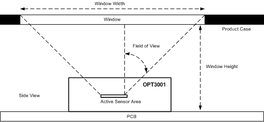
OPT3001-Q1 aij_Window_App_Diag_w_PCB.gifFigure 34. Product Case and Window Over the OPT3001-Q1 Device