SBOS293H December 2003 – December 2015 OPA695
PRODUCTION DATA.
- 1 Features
- 2 Applications
- 3 Description
- 4 Revision History
- 5 Pin Configuration and Functions
- 6 Specifications
- 7 Parameter Measurement Information
-
8 Detailed Description
- 8.1 Overview
- 8.2 Functional Block Diagram
- 8.3 Feature Description
- 8.4 Device Functional Modes
- 9 Application and Implementation
- 10Power Supply Recommendations
- 11Layout
- 12Device and Documentation Support
- 13Mechanical, Packaging, and Orderable Information
封装选项
机械数据 (封装 | 引脚)
散热焊盘机械数据 (封装 | 引脚)
- DGK|8
订购信息
9 Application and Implementation
NOTE
Information in the following applications sections is not part of the TI component specification, and TI does not warrant its accuracy or completeness. TI’s customers are responsible for determining suitability of components for their purposes. Customers should validate and test their design implementation to confirm system functionality.
9.1 Application Information
9.1.1 SAW Filter Buffer
One common requirement in an IF strip is to buffer the output of a mixer with enough gain to recover the insertion loss of a narrowband SAW filter. Figure 65 shows one possible configuration driving a SAW filter. Figure 53 shows the intercept at the 50-Ω load. Operating in the inverting mode at a voltage gain of –8 V/V, this circuit provides a 50-Ω input match using the gain set resistor, has the feedback optimized for maximum bandwidth (700 MHz in this case), and drives through a 50-Ω output resistor into the matching network at the input of the SAW filter. If the SAW filter gives a 12-dB insertion loss, a net gain of 0 dB to the 50-Ω load at the output of the SAW (which could be the input impedance of the next IF amplifier or mixer) is delivered in the passband of the SAW filter. Using the OPA695 in this application isolates the first mixer from the impedance of the SAW filter and provides very low two-tone, 3rd-order spurious levels in the SAW filter bandwidth. Inverting operation gives the broadest bandwidth up to a gain of –12 V/V (15.6 dB). Noninverting operation gives higher bandwidth at gain settings higher than this, but will also give a slight reduction in intercept and noise figure performance.
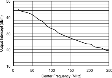 Figure 53. 2-Tone, 3rd-Order Intermodulation Intercept
9.1.2 LO Buffer Amplifier
The OPA695 can also be used to buffer the Local Oscillator (LO) from the mixer. Operating at a voltage gain of +2, the OPA695 provides almost perfect load isolation for the LO, with a net gain of 0 dB to the mixer. Applications through 1.4-GHz LOs may be considered, but best operation would be for LOs < 1.0 GHz at a gain of +2. Gain can also be provided by the OPA695 to drive higher power levels into the mixer. One option for the OPA695 as an LO buffer is shown in Figure 54. Because the OPA695 can drive multiple output loads, two identical LO signals may be delivered to the mixers in a diversity receiver by tapping the output off through two series 50-Ω output resistors. This circuit is set up for a voltage gain of +2 V/V to the output pin for a gain of +1 V/V (0 dB) to the mixers, but could easily be adjusted to deliver higher gains as well.
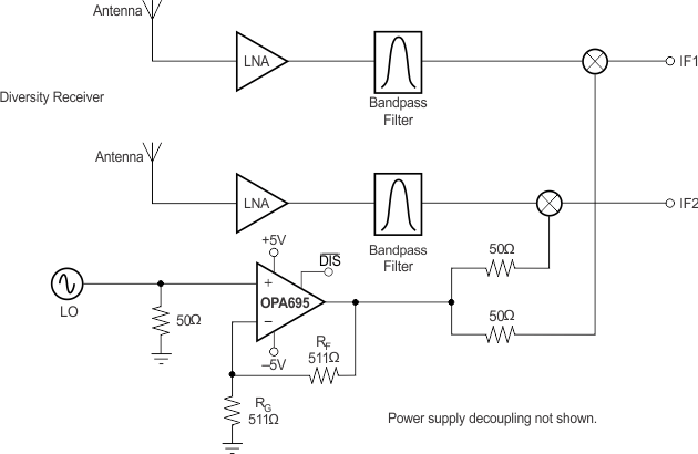 Figure 54. Dual Output LO Buffer
9.1.3 Wideband Cable Driving Applications
The high slew rate and bandwidth of the OPA695 can be used to meet the most demanding cable driving applications.
9.1.3.1 Cable Modem Return Path Driver
The standard cable modem upstream driver is typically required to drive high power over a 5-MHz to 65-MHz bandwidth while delivering < –50-dBc distortion. Highly-integrated solutions (including programmable gain stages) often fall short of this target due to high losses from the amplifier output to the line. The higher gain-operating capability of the OPA695 and its very high slew rate provide a low-cost solution for delivering this signal with the required spurious-free dynamic range. Figure 55 shows one example of using the OPA695 as an upstream driver for a cable modem return path. In this case, the input impedance of the driver is set to 75 Ω by the gain resistor (RG). The required input level from the adjustable gain stage is significantly reduced by the 15.5-dB gain provided by the OPA695. In this example, the physical 75-Ω output matching resistor, along with the 3-dB loss in the diplexer, attenuate the output swing by 9 dB on the line. In this example, a single +12-V supply was used to achieve the lowest harmonic distortion for the 6-VPP output pin voltage through 65 MHz. Measured performance for this example gave 600-MHz small-signal bandwidth and < –54-dBc distortion through 65 MHz for a 6-VPP output pin voltage swing.
An alternative to this circuit that gives even lower distortion is a differential driver using two OPA695s driving into an output transformer. This can be used either to double the available line power, or to improve distortion by cutting the required output swing in half for each stage. The channel disable required by the MCNS specification must be implemented by using the PGA disable feature. The MCNS disable specification requires that an output impedance match be maintained with the signal channel shut off. The disable feature of the OPA695 is intended principally for power savings and puts the output and inverting input pins into a high impedance mode. This does not maintain the required output-impedance matching. Turning off the signal at the input of Figure 55, while keeping the OPA695 active, maintains the impedance matching while putting very little noise on the line. The line noise in disable for the circuit of Figure 55 (with the PGA source turned off, but still presenting a 75-Ω source impedance) will be a very low 4 nV/√Hz (–157 dBm/Hz) due to the low input noise of the OPA695.
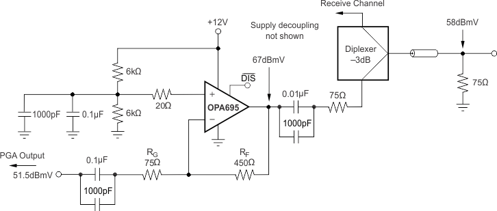 Figure 55. Cable Modem Upstream Driver
9.1.3.2 RGB Video Line Driver
The extremely high bandwidth of the OPA695 operating at a gain of +2 supports the fastest RAMDAC outputs for applications such as auxiliary monitor driving. Gain 2V/V Video Line Driver shows measured performance for a
0 → +1-V input square wave at 125 MHz. As a general rule, the required full-power bandwidth for the amplifier must be at least one-half the pixel rate. With its noninverting gain of +2, slew rate of 2900 V/μs, and a 1.4-VPP output pin voltage swing for standard RGB video levels, the OPA695 gives a bandwidth of 600 MHz, which then supports up to 1.26-GHz pixel rates. Figure 56 shows an example where three OPA695s provide an auxiliary monitor output for a highresolution RGB RAMDAC.
An alternative circuit that takes advantage of the higher inverting slew rate of the OPA695 (4300 V/μs) takes the complementary current output from the RAMDAC and converts it to positive video to give a very high, full-power bandwidth RGB line driver. This will give sharper pixel edges than the circuit of Figure 56. Most high-speed DACs are current-steering designs with both an output current signal used for the video, and a complementary output that is typically discarded into a matching resistor. The complementary current output can be used as an auxiliary output if it is inverted, as shown in Figure 57. In the circuit of Figure 57, the complementary current output is terminated by an equivalent 75-Ω impedance (the parallel combination of RT and RG) that also provides a current division to reduce the signal current through the feedback resistor, RF. This allows RF to be increased to a value which holds a flat frequency response. Since the complementary current output is essentially an inverted video signal, this circuit sets up a white video level at the output of the OPA695 for zero DAC output current (using the 0.77-V DC bias on the noninverting input), then inverts the complementary output current to produce a signal that ranges from this 1.4 V at zero output current down to 0 V at maximum output current level (assuming a 20-mA maximum output current). This gives a very wideband (> 800-MHz) video signal capability.
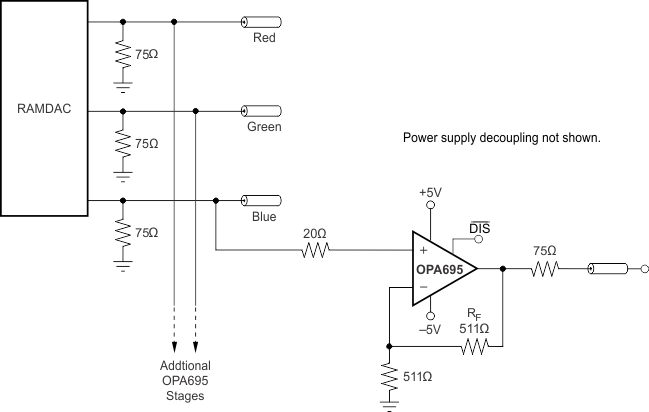 Figure 56. Gain of +2, High-Resolution RGB Monitor Output
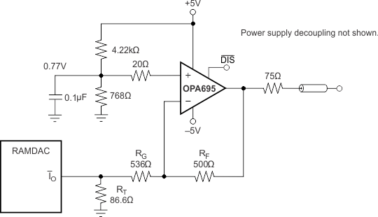 Figure 57. High-Resolution RGB Driver Using DAC Complementary Output Current
9.1.3.3 Arbitrary Waveform Driver
The OPA695 can be used as the output stage for moderate output power arbitrary waveform driver applications. Driving out through a series 50-Ω matching resistor into a 50-Ω matched load allows up to a 4.0-VPP swing at the matched load (15 dBm) when operating the OPA695 on a ±5-V power supply. This level of power is available for gains of either ±8 with a flat response through 100 MHz. When interfacing directly from a complementary current output DAC, consider the circuit of Figure 57, modified for the peak output currents of the particular DAC being considered. Where purely AC-coupled output signals are required from a complementary current output DAC, consider a push-pull output stage using the circuit of Figure 58. The resistor values here have been calculated for a 20-mA peak output current DAC, which produces up to a 5-VPP swing at the matched load (18 dBm). This approach gives higher power at the load, with lower 2nd-harmonic distortion.
For a 20-mA peak output current DAC, the mid-scale current of 10 mA gives a 2-V DC output common-mode operating voltage, due to the 200-Ω resistor to ground at the outputs. The total AC impedance at each output is 50 Ω, giving a ±0.5-V swing around this 2-V common-mode voltage for the DAC. These resistors also act as a current divider, sending 75% of the DAC output current through the feedback resistor (464 Ω). The blocking capacitor references the OPA695 output voltage to ground, and turns the unipolar DAC output current into a bipolar swing of 0.75 × 20 mA × 464 Ω = 7 VPP at each amplifier output. Each output is exactly 180° out-of-phase from the other, producing double 7 VPP into the matching resistors. To limit the peak output current and improve distortion, the circuit of Figure 58 is set up with a 1.4:1 stepdown transformer. This reflects the 50-Ω load to be 100 Ω at the primary side of the transformer. For the maximum 14-VPP swing across the outputs of the two amplifiers, the matching resistors will drop this to 7 VPP at the input of the transformer, then down to 5-VPP maximum at the 50-Ω load at the output of the transformer. This step-down approach reduces the peak output current to 14 VP/(200 Ω) = 70 mA.
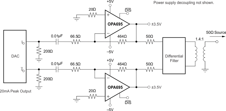 Figure 58. High Power, Wideband AC-Coupled Arbitrary Waveform Driver
9.1.4 Differential I/O Applications
The OPA695 offers very low 3rd-order distortion terms with a dominant 2nd-order distortion for the single amplifier operation. For the lowest distortion, particularly where differential outputs are needed, operating two OPA695s in a differential I/O design suppresses these even-order terms, delivering extremely low harmonic distortion through high frequencies and powers. Differential outputs are often preferred for high performance ADCs, twisted-pair driving, and mixer interfaces. Two basic approaches to differential I/Os are the noninverting or inverting configurations. Because the output is differential, the signal polarity is somewhat meaningless; the noninverting and inverting terminology applies here to where the input is brought into the two OPA695s. Each approach has its advantages and disadvantages. Figure 59 shows a basic starting point for non-inverting differential I/O applications.
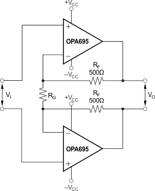 Figure 59. Noninverting Input Differential I/O Amplifier
This approach allows for a source termination impedance independent of the signal gain. For instance, simple differential filters may be included in the signal path right up to the non-inverting inputs without interacting with the gain setting. The differential signal gain for the circuit of Figure 59 is:
Because the OPA695 is a current feedback amplifier, its bandwidth is principally controlled with the feedback resistor value: Figure 59 shows a typical value of 500 Ω. However, the differential gain may be adjusted with considerable freedom using just the RG resistor. RG can be a reactive network providing an isolated shaping to the differential frequency response. AC-coupled applications often include a blocking capacitor in series with RG. This reduces the gain to 1 at low frequency, rising to the AD expression shown above at higher frequencies. The noninverting input approach of Figure 59 can be used for higher gains than the inverting input approach, but may have a reduced full-power bandwidth due to the lower slew rate of the OPA695 running a noninverting versus inverting input mode of operation.
Various combinations of single-supply or AC-coupled gain can also be delivered using the basic circuit of Figure 59. Common-mode bias voltages on the two noninverting inputs pass on to the output with a gain of 1, as an equal DC voltage at each inverting node creates no current through RG. This circuit shows a common-mode gain of 1 from input to output. The source connection must either remove this common-mode signal if it is unnecessary (using an input transformer), or the common-mode voltage at the inputs can set the output common-mode bias. If the low common-mode rejection of this circuit is a problem, the output interface may also be used to reject that common-mode. For instance, most modern differential input ADCs reject common-mode signals well, while a line driver application through a transformer also removes the common-mode signal at the secondary of the transformer.
Figure 60 shows a differential I/O stage configured as an inverting amplifier. In this case, the gain resistors (RG) become part of the input resistance for the source. This provides a better noise performance than the non-inverting configuration, but limits the flexibility in setting the input impedance separately from the gain.
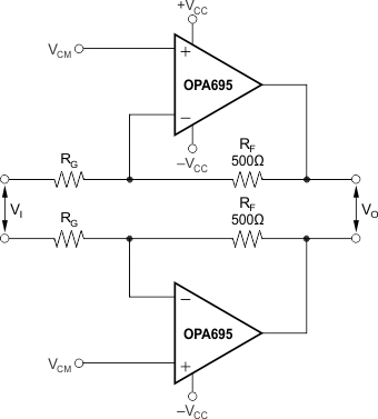 Figure 60. Inverting Input Differential I/O Amplifier
The two noninverting inputs provide an easy common-mode control input, particularly if the source is AC-coupled through either blocking caps or a transformer. In either case, the common-mode input voltages on the two noninverting inputs again have a gain of 1 to the output pins, giving easy common-mode control for single-supply operation. The OPA695 in this configuration constrains the feedback to the 500-Ω region for best frequency response. With RF fixed, the input resistors may be adjusted to the desired gain, but will also be changing the input impedance. The high-frequency common-mode gain for this circuit from input to output is the same as for the signal gain. Again, if the source might include an undesired common-mode signal, that could be rejected at the input using blocking caps (for low-frequency and DC common-mode) or a transformer coupling. The differential performance plots shown in the Typical Characteristics used the configuration of Figure 60 and an input 1:1 transformer. The differential signal gain in the circuit of Figure 60 is:
Using this configuration suppresses the 2nd-harmonics, leaving only 3rd-harmonic terms as the limit to output SFDR. The higher slew rate of the inverting configuration also extends the full-power bandwidth and the range of low intermodulation distortion over the performance bandwidth available from the circuit of Figure 59. The Typical Characteristics show that the circuit of Figure 60 operating at an AD = 10 can deliver a 16 VPP signal with over 500-MHz –3-dB bandwidth. Using Equation 4, this implies a differential output slew of 18000 V/μsec, or 9000 V/μsec at each output. This output slew rate is far higher than specified, and probably due to the lighter load used in the differential tests.
This inverting input differential configuration is suited to high SFDR converter interfaces, specifically narrowband IF channels. The Typical Characteristics show the 2-tone, 3rd-order intermodulation intercept exceeding 45 dBm through 90 MHz. Although this data was taken with an 800-Ω load, the intercept model appears to work for this circuit, treating the power level as if it were into 50 Ω. For example, at 70 MHz, the differential Typical Characteristic plots show a 48 dBm intercept. To predict the 2-tone intermodulation SFDR, assuming a –1-dB below full-scale envelope to a 2-VPP maximum differential input converter, the test power level would be 9 dBm – 6 dBm = 3 dBm for each tone. Putting this into the intercept equation, gives:
The single-tone distortion data shows approximately 72-dB SFDR at 70 MHz for a 2-VPP output into this light 800-Ω load. A modest post filter after the amplifier can reduce these harmonics (2nd at 140 MHz, 3rd at 210 MHz) to the point where the full SFDR to a converter can be in the 85-dB range for a 70-MHz IF operation.
9.1.5 Operating Suggestions
9.1.5.1 Setting Resistor Values to Optimize Bandwidth
A current-feedback operational amplifier such as the OPA695 can hold an almost constant bandwidth over signal gain settings with the proper adjustment of the external resistor values. This is shown in Typical Characteristics. The small-signal bandwidth decreases only slightly with increasing gain. These curves also show that the feedback resistor has been changed for each gain setting. The resistor values on the inverting side of the circuit for a current-feedback operational amplifier can be treated as frequency response compensation elements, while their ratios set the signal gain. Figure 15 shows the analysis circuit for the OPA695 small-signal frequency response.
The key elements of this current feedback operational amplifier model are:
- α ⇒ Buffer gain from the noninverting input to the inverting input.
- RI ⇒ Buffer output impedance
- iERR ⇒ Feedback error current signal
- Z(s) ⇒ Frequency-dependent, open-loop transimpedance gain from iERR to VO
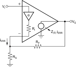 Figure 61. Current-Feedback Transfer Function Analysis Circuit
The buffer gain is typically very close to 1.00 and is normally neglected from signal gain considerations. It will, however, set the CMRR for a single operational amplifier differential amplifier configuration. For the buffer gain α < 1.0, the CMRR = –20 × log (1 – α).
RI, the buffer output impedance, is a critical portion of the bandwidth control equation. For the OPA695, it is typically about 28 Ω for ±5-V operation, and 31 Ω for single +5-V operation.
A current-feedback operational amplifier senses an error current in the inverting node (as opposed to a differential input error voltage for a voltage-feedback operational amplifier) and passes this on to the output through an internal frequency-dependent transimpedance gain. Typical Characteristics show this open-loop transimpedance response. This is analogous to the open-loop voltage gain curve for a voltage-feedback operational amplifier. Developing the transfer function for the circuit of Figure 64 gives Equation 9:
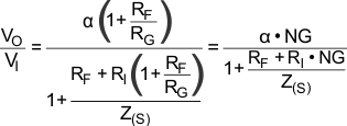
where
- NC = 1 + RF/RG = Noise Gain
This is written in a loop gain analysis format, where the errors arising from a non-infinite open-loop gain are shown in the denominator. If Z(s) were infinite over all frequencies, the denominator of Equation 9 would reduce to 1, and the ideal desired signal gain shown in the numerator would be achieved. The fraction in the denominator of Equation 9 determines the frequency response. Equation 10 shows this as the loop gain equation:

If 20 × log (RF + NG × RI) were superimposed on the open-loop transimpedance plot, the difference between the two would be the loop gain at a given frequency. Eventually, Z(s) rolls off to equal the denominator of Equation 10, at which point the loop gain has reduced to 1 (and the curves have intersected). This point of equality is where the amplifier closed-loop frequency response given by Equation 9 starts to roll off, and is exactly analogous to the frequency at which the noise gain equals the open-loop voltage gain for a voltage-feedback operational amplifier. The difference is that the total impedance in the denominator of Equation 10 may be controlled separately from the desired signal gain (or NG).
The OPA695 is internally compensated to give a maximally flat frequency response for RF = 402 Ω at NG = 8 on ±5-V supplies. Evaluating the denominator of Equation 7 (the feedback transimpedance) gives an optimal target of 663 Ω. As the signal gain changes, the contribution of the NG ×RI term in the feedback transimpedance changes, but the total can be held constant by adjusting RF. Equation 11 gives an approximate equation for optimum RF over signal gain:
As the desired signal gain increases, this equation will eventually predict a negative RF. A subjective limit to this adjustment can be set by holding RG to a minimum value of 10 Ω. Lower values will load both the buffer stage at the input and the output stage if RF gets too low, decreasing the bandwidth. Figure 62 shows the recommended RF versus NG for both ±5 V and a single +5-V operation. The optimum target feedback impedance for +5-V operation used in Equation 8 is 663 Ω, while the typical buffer output impedance is 32 Ω. The values for RF versus gain shown are approximately equal to the values used to generate the typical characteristic curves. In some cases, the values used differ slightly from that shown here, in that the values used in the typical characteristics are also correcting for board parasitics not considered in the simplified analysis leading to Equation 11. The values shown in Figure 62 give a good starting point for designs where bandwidth optimization is desired and a flat frequency response is needed.
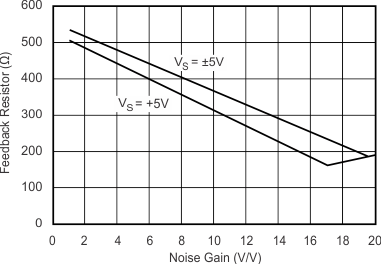 Figure 62. Recommended Feedback Resistor vs Noise Gain
The total impedance presented to the inverting input can adjust the closed-loop signal bandwidth. Inserting a series resistor between the inverting input and the summing junction increases the feedback impedance (denominator of Equation 10), decreasing the bandwidth. The internal buffer output impedance for the OPA695 is slightly influenced by the source impedance looking out of the noninverting input terminal. High source resistors increase RI, decreasing the bandwidth. For those single-supply applications which develop a midpoint bias at the non-inverting input through high-valued resistors, the decoupling capacitor is essential for power-supply ripple rejection, non-inverting input noise current shunting, and minimizing the high-frequency value for RI in Figure 61.
Inverting feedback optimization is complicated by the impedance matching requirement at the input, as shown in Figure 49. The resistor values shown in Table 3 must be used in this case.
9.1.5.2 Output Current and Voltage
The OPA695 provides output voltage and current capabilities consistent with driving doubly-terminated 50-Ω lines. For a 100-Ω load at a gain of +8 (see Figure 48), the total load is the parallel combination of the 100-Ω load and the 456-Ω total feedback network impedance. This 82-Ω load requires no more than 45-mA output current to support the ±3.7-V minimum output voltage swing specified for 100-Ω loads. This is well below the minimum ±90-mA specifications.
The specifications described above, though familiar in the industry, consider voltage and current limits separately. In many applications, it is the voltage × current, or V-I, product which is more relevant to circuit operation. Refer to Figure 21. The X and Y axes of this graph show the zero-voltage output current limit and the zero-current output voltage limit, respectively. The four quadrants provide a more detailed view of the OPA695 output drive capabilities. Superimposing resistor load lines onto the plot shows the available output voltage and current for specific loads.
The minimum specified output voltage and current overtemperature are set by worst-case simulations at the cold temperature extreme. Only at cold startup does the output current and voltage decrease to the numbers shown in the specification tables. As the output transistors deliver power, the junction temperatures increase, decreasing the VBEs (increasing the available output voltage swing) and increasing the current gains (increasing the available output current). In steady-state operation, the available output voltage and current are always be greater than that shown in the over-temperature specifications, because the output stage junction temperatures are higher than the minimum specified operating ambient.
To maintain maximum output-stage linearity, no output short-circuit protection is provided. This is not normally a problem, as most applications include a series-matching resistor at the output that limits the internal power dissipation if the output side of this resistor is shorted to ground. However, shorting the output pin directly to the adjacent positive power supply pin will, in most cases, destroy the amplifier. If additional short-circuit protection is required, consider a small series resistor in the power-supply leads. Under heavy output loads, this reduces the available output voltage swing. A 5-Ω series resistor in each power-supply lead limits the internal power dissipation to less than 1W for an output short circuit, while decreasing the available output voltage swing only 0.25 V for up to 50-mA desired load currents. Always place the 0.1-μF power supply decoupling capacitors directly on the supply pins after these supply current-limiting resistors.
9.1.5.3 Driving Capacitive Loads
One of the most demanding, and yet very common, load conditions for an operational amplifier is capacitive loading. Often, the capacitive load is the input of an A/D converter,including additional external capacitance which may be recommended to improve A/D linearity. A high-speed, high open-loop gain amplifier like the OPA695 can be susceptible to decreased stability and closed-loop response peaking when a capacitive load is placed directly on the output pin. When the open-loop output resistance of the amplifier is considered, this capacitive load introduces an additional pole in the signal path that can decrease the phase margin. Several external solutions to this problem have been suggested. When the primary considerations are frequency response flatness, pulse response fidelity, and distortion, the simplest and most effective solution is to isolate the capacitive load from the feedback loop by inserting a series isolation resistor between the amplifier output and the capacitive load. This does not eliminate the pole from the loop response, but shifts it and adds a zero at a higher frequency. The additional zero acts to cancel the phase lag from the capacitive load pole, thus increasing the phase margin and improving stability.
The typical characteristics show the recommended RS versus capacitive load and the resulting frequency response at the load. Parasitic capacitive loads greater than 2 pF can begin to degrade the performance of the OPA695. Long PCB traces, unmatched cables, and connections to multiple devices can exceed this value. Always consider this effect carefully and add the recommended series resistor as close as possible to the OPA695 output pin (see Layout Guidelines).
9.1.5.4 Distortion Performance
The OPA695 provides good distortion performance into a 100-Ω load on ±5-V supplies. Compared to other solutions, the OPA695 holds lower distortion at higher frequencies (> 20 MHz). Generally, until the fundamental signal reaches very high frequency or power levels, the 2nd-harmonic dominates the distortion with a negligible 3rd-harmonic component. Focusing on the 2nd-harmonic, increasing the load impedance directly improves distortion: the total load includes the feedback network. In the non-inverting configuration (see Figure 48), this is the sum of RF + RG, while in the inverting configuration, it is only RF. Also, providing an additional supply decoupling capacitor (0.01 μF) between the supply pins (for bipolar operation) improves the 2nd-order distortion slightly (3 dB to 6 dB).
In most operational amplifiers, increasing the output voltage swing directly increases harmonic distortion. The typical performance curves show the 2nd-harmonic increasing at a little less than the expected 2x rate, while the 3rd-harmonic increases at a little less than the expected 3x rate. Where the test power doubles, the difference between it and the 2nd harmonic decreases less than the expected 6 dB, while the difference between it and the 3rd decreases by less than the expected 12 dB.
The OPA695 has extremely low 3rd-order harmonic distortion. This also gives a high 2-tone, 3rd-order intermodulation intercept, as shown in the typical characteristic curves. This intercept curve is defined at the 50-Ω load when driven through a 50-Ω matching resistor to allow direct comparisons to RF MMIC devices, and is shown for both gains of ±8. There is a slight improvement in intercept by operating the OPA695 in the inverting mode. The output matching resistor attenuates the voltage swing from the output pin to the load by 6 dB. If the OPA695 drives directly into the input of a high impedance device, such as an ADC, this 6-dB attenuation is not taken. Under these conditions, the intercept increases by a minimum 6 dBm.
The intercept predicts the intermodulation products for two closely-spaced frequencies. If the two test frequencies, F1 and F2, are specified in terms of average and delta frequency, FO = (F1 + F2)/2 and ΔF = |F2 – F1| /2, the two 3rd-order, close-in spurious tones will appear at FO ±3 × ΔF. The difference between two equal test-tone power levels and these intermodulation spurious power levels is given by ΔdBc = 2 × (OP3 – PO), where OP3 is the intercept taken from the typical characteristic curve and PO is the power level in dBm at the 50-Ω load for one of the two closely-spaced test frequencies. For example, at 50 MHz, gain of –8, the OPA695 has an intercept of 42 dBm at a matched 50-Ω load. If the full envelope of the two frequencies must be 2 VPP, this requires each tone to be 4 dBm. The 3rd-order intermodulation spurious tones are then 2 × (42 – 4) = 76 dBc below the test-tone power level (–72 dBm). If this same 2-VPP 2-tone envelope were delivered directly into the input of an ADC without the matching loss or the loading of the 50-Ω network, the intercept would increase to at least 48 dBm. With the same signal and gain conditions, but now driving directly into a light load, the 3rd-order spurious tones are then at least 2 × (48 – 4) = 88 dBc below the 4-dBm test-tone power levels centered on 50 MHz. Tests have shown that, in reality, the 3rd-order spurious levels are much lower due to the lighter loading presented by most ADCs.
9.1.5.5 Noise Performance
The OPA695 offers an excellent balance between voltage and current noise terms to achieve low output noise. The inverting current noise (22 pA/√Hz) is lower than most other current-feedback operational amplifiers, while the input voltage noise (1.8 nV/√Hz) is lower than any unity-gain stable, wideband, voltage-feedback operational amplifier. This low-input voltage noise was achieved at the price of a higher noninverting input current noise (18 pA/√Hz). As long as the AC source impedance looking out of the noninverting node is less than 50 Ω, this current noise does not contribute significantly to the total output noise. The operational amplifier input voltage noise and the two input current noise terms combine to give low output noise under a wide variety of operating conditions. Figure 63 shows the operational amplifier noise analysis model with all the noise terms included. In this model, all noise terms are taken to be noise voltage or current density terms in either nV/√Hz or pA/√Hz.
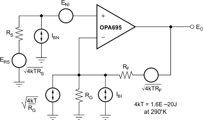 Figure 63. Operational Amplifier Noise Figure Analysis Model
The total output spot-noise voltage can be computed as the square root of the sum of all squared output noise voltage contributors. Equation 12 shows the general form for the output noise voltage using the terms shown in Figure 59.

Dividing this expression by the noise gain (NG = (1 + RF/RG)) gives the equivalent input referred spot-noise voltage at the noninverting input, as shown in Equation 13:

Evaluating these two equations for the OPA695 circuit and component values shown in Figure 48 gives a total output spot-noise voltage of 18.7 nV/√Hz and a total equivalent input spot-noise voltage of 2.3 nV/√Hz. This total input referred spot-noise voltage is higher than the 1.8-nV/√Hz specification for the operational amplifier voltage noise alone. This reflects the noise added to the output by the inverting current noise times the feedback resistor. If the feedback resistor is reduced in high-gain configurations (as suggested previously), the total input referred voltage noise given by Equation 13 just approaches the 1.8 nV/√Hz of the operational amplifier itself. For example, going to a gain of +20 (using RF = 200 Ω) gives a total input referred noise of 2.0 nV/√Hz.
For a more complete discussion of operational amplifier noise calculation, see TI Application Note, SBOA066, Noise Analysis for High Speed Op Amps, available through www.ti.com.
9.1.5.6 DC Accuracy and Offset Control
A current-feedback operational amplifier such as the OPA695 provides exceptional bandwidth in high gains, giving fast pulse settling but only moderate DC accuracy. The typical specifications show an input offset voltage comparable to high-speed voltage-feedback amplifiers; however, the two input bias currents are somewhat higher and are unmatched. Although bias current cancellation techniques are effective with most voltage-feedback operational amplifiers, they do not generally reduce the output DC offset for wideband current-feedback operational amplifiers. Because the two input bias currents are unrelated in both magnitude and polarity, matching the source impedance looking out of each input to reduce their error contribution to the output is ineffective. Evaluating the configuration of Figure 48, using a worst-case +25°C input offset voltage and the two input bias currents, gives a worst-case output offset range equal to:
where
- NG = noninverting signal gain
= ±(8 × 3.0 mV) ± (30 µA × 25 Ω × 8) ±(402 Ω × 60 µA)
= ±24 mV ± 1.6 mV ± 24 mV
= ±54 mV
A fine-scale output offset null, or DC operating point adjustment, is often required. Numerous techniques are available for introducing DC offset control into an operational amplifier circuit. Most simple adjustment techniques do not correct for temperature drift.
9.1.5.7 Power Shutdown Operation
The OPA695 provides an optional power shutdown feature that can be used to reduce system power. If the VDIS control pin is left unconnected, the OPA695 operates normally. This shutdown is intended only as a power-saving feature. Forward path isolation is effective for small signals. Large signal isolation is not ensured. Using this feature to multiplex two or more outputs together is not recommended. Large signals applied to the shutdown output stages can turn on parasitic devices, degrading signal linearity for the desired channel.
Turn-on time is quick from the shutdown condition, typically < 60 ns. Turn-off time is strongly dependent on the external circuit configuration, but is typically 200 ns for the circuit of Figure 48.
To shut down, the control pin must be asserted low. This logic control is referenced to the positive supply, as shown in the simplified circuit of Figure 64.
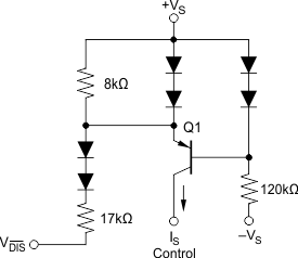 Figure 64. Operational Amplifier Noise Figure Analysis Model
In normal operation, base current to Q1 is provided through the 120-kΩ resistor, while the emitter current through the 8-kΩ resistor sets up a voltage drop that is inadequate to turn on the two diodes in the Q1 emitter. As VDIS is pulled low, additional current is pulled through the 8-kΩ resistor, eventually turning on these two diodes (≈ 180 μA). At this point, any further current pulled out of VDIS goes through those diodes holding the emitter-base voltage of Q1 at approximately 0 V. This shuts off the collector current out of Q1, turning the amplifier off. The supply current in the shutdown mode is only that required to operate the circuit of Figure 64.
When disabled, the output and input nodes go to a high impedance state. If the OPA695 is operating in a gain of +1, this will show a very high impedance (3 pF || 1 MΩ) at the output and exceptional signal isolation. If operating at a gain greater than +1, the total feedback network resistance (RF + RG) appears as the impedance looking back into the output, but the circuit will still show very high forward and reverse isolation. If configured as an inverting amplifier, the input and output are connected through the feedback network resistance (RF + RG), giving relatively poor input to output isolation.
9.1.5.8 Thermal Analysis
The OPA695 does not require external heatsinking for most applications. Maximum desired junction temperature sets the maximum allowed internal power dissipation as described below. In no case should the maximum junction temperature be allowed to exceed 150°C.
Operating junction temperature (TJ) is given by TA + PD × θJA. The total internal power dissipation (PD) is the sum of quiescent power (PDQ) and additional power dissipated in the output stage (PDL) to deliver load power. Quiescent power is simply the specified no-load supply current times the total supply voltage across the part. PDL depends on the required output signal and load. However, for a grounded resistive load, PDL would be at a maximum when the output is fixed at a voltage equal to one-half of either supply voltage (for equal bipolar supplies). Under this condition, PDL = VS 2/(4 × RL), where RL includes feedback network loading.
Note that it is the power in the output stage and not into the load that determines internal power dissipation.
As an absolute worst-case example, compute the maximum TJ using an OPA695IDBV (SOT23-6 package) in the circuit of Figure 48 operating at the maximum specified ambient temperature of +85°C and driving a grounded 100-Ω load.
This maximum operating junction temperature is well below most system level targets. Most applications are lower as an absolute worst-case output stage power was assumed in this calculation.
9.2 Typical Application
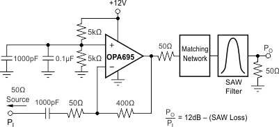 Figure 65. IF Amplifier Driving SAW Filter
9.2.1 Design Requirements
9.2.1.1 Saw Filter Buffer
One common requirement in an IF strip is to buffer the output of a mixer with enough gain to recover the insertion loss of a narrowband SAW filter. Figure 65 shows one possible configuration driving a SAW filter. Figure 53 shows the intercept at the 50-Ω load. Operating in the inverting mode at a voltage gain of –8 V/V, this circuit provides a 50-Ω input match using the gain set resistor, has the feedback optimized for maximum bandwidth (700 MHz in this case), and drives through a 50-Ω output resistor into the matching network at the input of the SAW filter. If the SAW filter gives a 12-dB insertion loss, a net gain of 0 dB to the 50-Ω load at the output of the SAW (which could be the input impedance of the next IF amplifier or mixer) is delivered in the passband of the SAW filter. Using the OPA695 in this application isolates the first mixer from the impedance of the SAW filter and provides very low two-tone, 3rd-order spurious levels in the SAW filter bandwidth. Inverting operation gives the broadest bandwidth up to a gain of –12 V/V (15.6 dB). Noninverting operation gives higher bandwidth at gain settings higher than this, but will also give a slight reduction in intercept and noise figure performance.
9.2.2 Detailed Design Procedure
The design procedure begins with calculating the required signal gain and signal swing. Once the gain and swing requirements are determined the appropriate amplifier is selected along with the required supply voltage. Due to the input impedance of 50 Ω the gain and the input impedance require a feedback resistor value of 400 Ω.
In this application the supply voltage is 12 V single ended. In order to provide the proper DC operating point it is necessary to apply a mid supply voltage to the non inverting input. This is accomplished by using a resistive voltage divider composed of two 1% precision 5-kΩ resistors along with two ceramic bypass capacitors. These components provide an accurate and low AC impedance reference voltage for the non inverting input. The inverting input requires only an AC coupling capacitor to isolate the 6 V operating voltage from the signal source. In this example a ceramic 1000-pF capacitor is used.
The circuit shown in Figure 65 shows an output resistor value of 50 Ω. This resistor will need to be adjusted to accommodate the SAW input impedance. Additional L/C components may be required as well, consult the SAW manufacturer's design guidelines for more details.
9.2.3 Application Curve
 Figure 66. 2-Tone, 3rd-Order Intermodulation Intercept