SBOS432G August 2008 – August 2016 OPA2330 , OPA330 , OPA4330
PRODUCTION DATA.
- 1 Features
- 2 Applications
- 3 Description
- 4 Revision History
- 5 Device Comparison Table
- 6 Pin Configurations and Functions
- 7 Specifications
- 8 Detailed Description
- 9 Application and Implementation
- 10Power Supply Recommendations
- 11Layout
- 12Device and Documentation Support
- 13Mechanical, Packaging, and Orderable Information
封装选项
请参考 PDF 数据表获取器件具体的封装图。
机械数据 (封装 | 引脚)
- D|14
- RGY|14
- PW|14
散热焊盘机械数据 (封装 | 引脚)
- RGY|14
订购信息
9 Application and Implementation
NOTE
Information in the following applications sections is not part of the TI component specification, and TI does not warrant its accuracy or completeness. TI’s customers are responsible for determining suitability of components for their purposes. Customers should validate and test their design implementation to confirm system functionality.
9.1 Application Information
The OPA330, OPA2330, and OPA4330 are unity-gain stable, precision operational amplifiers free from unexpected output and phase reversal. The use of proprietary Zerø-Drift circuitry gives the benefit of low input offset voltage over time and temperature, as well as lowering the 1/f noise component. As a result of the high PSRR, these devices work well in applications that run directly from battery power without regulation. The OPA330 family is optimized for low-voltage, single-supply operation. These miniature, high-precision, low quiescent current amplifiers offer high-impedance inputs that have a common-mode range 100 mV beyond the supplies and a rail-to-rail output that swings within 100 mV of the supplies under normal test conditions. The OPA330 series are precision amplifiers for cost-sensitive applications.
9.1.1 Operating Voltage
The OPA330 series operational amplifiers can be used with single or dual supplies from an operating range of
VS = 1.8 V (±0.9 V) up to 5.5 V (±2.75 V). Supply voltages greater than 7 V can permanently damage the device (see Absolute Maximum Ratings). Key parameters that vary over the supply voltage or temperature range are shown in Typical Characteristics.
9.1.2 Input Voltage
The OPA330, OPA2330, and OPA4330 input common-mode voltage range extends 0.1 V beyond the supply rails. The OPA330 is designed to cover the full range without the troublesome transition region found in some other rail-to-rail amplifiers.
Typically, input bias current is approximately 200 pA. Input voltages exceeding the power supplies however, can cause excessive current to flow into or out of the input pins. Momentary voltages greater than the power supply can be tolerated if the input current is limited to 10 mA. This limitation is easily accomplished with an input resistor, as shown in Figure 18.
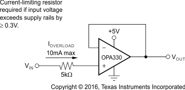 Figure 18. Input Current Protection
9.1.3 Input Differential Voltage
The typical input bias current of the OPA330 during normal operation is approximately 200 pA. In over-driven conditions, the bias current can increase significantly (see Figure 17). The most common cause of an over-driven condition occurs when the operational amplifier is outside of the linear range of operation. When the output of the operational amplifier is driven to one of the supply rails the feedback loop requirements cannot be satisfied and a differential input voltage develops across the input pins. This differential input voltage results in activation of parasitic diodes inside the front end input chopping switches that combine with 10-kΩ electromagnetic interference (EMI) filter resistors to create the equivalent circuit illustrated in Figure 19. Notice that the input bias current remains within specification within the linear region.
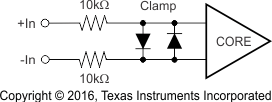 Figure 19. Equivalent Input Circuit
9.1.4 Internal Offset Correction
The OPA330, OPA2330, and OPA4330 operational amplifiers use an auto-calibration technique with a time-continuous, 125-kHz operational amplifier in the signal path. This amplifier is zero-corrected every 8 µs using a proprietary technique. Upon power up, the amplifier requires approximately 100 µs to achieve specified VOS accuracy. This design has no aliasing or flicker noise.
9.1.5 EMI Susceptibility and Input Filtering
Operational amplifiers vary in their susceptibility to EMI. If conducted EMI enters the operational amplifier, the DC offset observed at the amplifier output may shift from its nominal value while the EMI is present. This shift is a result of signal rectification associated with the internal semiconductor junctions. While all operational amplifier pin functions can be affected by EMI, the input pins are likely to be the most susceptible. The OPA330 operational amplifier family incorporates an internal input low-pass filter that reduces the amplifier response to EMI. Both common-mode and differential mode filtering are provided by the input filter. The filter is designed for a cutoff frequency of approximately 8 MHz (–3 dB), with a rolloff of 20 dB per decade.
9.1.6 Achieving Output Swing to the Operational Amplifier Negative Rail
Some applications require output voltage swings from 0 V to a positive full-scale voltage (such as 2.5 V) with excellent accuracy. With most single-supply operational amplifiers, problems arise when the output signal approaches 0 V, near the lower output swing limit of a single-supply operational amplifier. A good single-supply operational amplifier may swing close to single-supply ground, but does not reach ground. The output of the OPA330, OPA2330, and OPA4330 can be made to swing to ground, or slightly below, on a single-supply power source. To do so requires the use of another resistor and an additional, more negative, power supply than the operational amplifier negative supply. A pulldown resistor may be connected between the output and the additional negative supply to pull the output down below the value that the output would otherwise achieve, as shown in Figure 20.
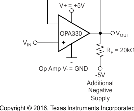 Figure 20. For VOUT Range to Ground
The OPA330, OPA2330, and OPA4330 have an output stage that allows the output voltage to be pulled to its negative supply rail, or slightly below, using the technique previously described. This technique only works with some types of output stages. The OPA330, OPA2330, and OPA4330 have been characterized to perform with this technique; the recommended resistor value is approximately 20 kΩ. This configuration increases the current consumption by several hundreds of microamps. Accuracy is excellent down to 0 V and as low as –2 mV. Limiting and nonlinearity occur below –2 mV, but excellent accuracy returns as the output is again driven above –2 mV. Lowering the resistance of the pulldown resistor allows the operational amplifier to swing even further below the negative rail. Resistances as low as 10 kΩ can be used to achieve excellent accuracy down to
–10 mV.
9.1.7 Photosensitivity
Although the OPA330 YFF package has a protective backside coating that reduces the amount of light exposure on the die, unless fully shielded, ambient light can reach the active region of the device. Input bias current for the package is specified in the absence of light. Depending on the amount of light exposure in a given application, an increase in bias current, and possible increases in offset voltage should be expected. Fluorescent lighting may introduce noise or hum because of the time-varying light output. Best layout practices include end-product packaging that provides shielding from possible light sources during operation.
9.2 Typical Application
9.2.1 Bidirectional Current-Sensing
This single-supply, low-side, bidirectional current-sensing solution detects load currents from –1 A to 1 A. The single-ended output spans from 110 mV to 3.19 V. This design uses the OPA2330 because of its low offset voltage and rail-to-rail input and output. One of the amplifiers is configured as a difference amplifier and the other provides the reference voltage.
Figure 21 shows the solution.
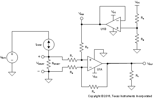 Figure 21. Bidirectional Current-Sensing Schematic
9.2.1.1 Design Requirements
This solution has the following requirements:
- Supply voltage: 3.3 V
- Input: –1 A to 1 A
- Output: 1.65 V ±1.54 V (110 mV to 3.19 V)
9.2.1.2 Detailed Design Procedure
The load current, ILOAD, flows through the shunt resistor (RSHUNT) to develop the shunt voltage, VSHUNT. The shunt voltage is then amplified by the difference amplifier, which consists of U1A and R1 through R4. The gain of the difference amplifier is set by the ratio of R4 to R3. To minimize errors, set R2 = R4 and R1 = R3. The reference voltage, VREF, is supplied by buffering a resistor divider using U1B. The transfer function is given by Equation 1.

where
There are two types of errors in this design: offset and gain. Gain errors are introduced by the tolerance of the shunt resistor and the ratios of R4 to R3 and, similarly, R2 to R1. Offset errors are introduced by the voltage divider (R5 and R6) and how closely the ratio of R4/R3 matches R2/R1. The latter value impacts the CMRR of the difference amplifier, which ultimately translates to an offset error.
Because this is a low-side measurement, the value of VSHUNT is the ground potential for the system load. Therefore, it is important to place a maximum value on VSHUNT. In this design, the maximum value for VSHUNT is set to 100 mV. Equation 2 calculates the maximum value of the shunt resistor given a maximum shunt voltage of 100 mV and maximum load current of 1 A.

The tolerance of RSHUNT is directly proportional to cost. For this design, a shunt resistor with a tolerance of 0.5% was selected. If greater accuracy is required, select a 0.1% resistor or better.
The load current is bidirectional; therefore, the shunt voltage range is –100 mV to 100 mV. This voltage is divided down by R1 and R2 before reaching the operational amplifier, U1A. Take care to ensure that the voltage present at the noninverting node of U1A is within the common-mode range of the device. Therefore, it is important to use an operational amplifier, such as the OPA330, that has a common-mode range that extends below the negative supply voltage. Finally, to minimize offset error, note that the OPA330 has a typical offset voltage of merely ±8 µV (±50 µV maximum).
Given a symmetric load current of –1 A to 1 A, the voltage divider resistors (R5 and R6) must be equal. To be consistent with the shunt resistor, a tolerance of 0.5% was selected. To minimize power consumption,
10-kΩ resistors were used.
To set the gain of the difference amplifier, the common-mode range and output swing of the OPA330 must be considered. Equation 3 and Equation 4 depict the typical common-mode range and maximum output swing, respectively, of the OPA330 given a 3.3-V supply.
The gain of the difference amplifier can now be calculated as shown in Equation 5.

The resistor value selected for R1 and R3 was 1 kΩ. 15.4 kΩ was selected for R2 and R4 because it is the nearest standard value. Therefore, the ideal gain of the difference amplifier is 15.4 V/V.
The gain error of the circuit primarily depends on R1 through R4. As a result of this dependence, 0.1% resistors were selected. This configuration reduces the likelihood that the design requires a two-point calibration. A simple one-point calibration, if desired, removes the offset errors introduced by the 0.5% resistors.
9.2.1.3 Application Curve
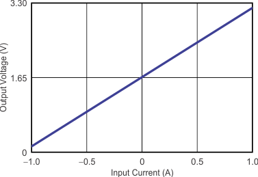
Output Voltage vs Input Current
9.3 System Examples
9.3.1 Single Operational Amplifier Bridge Amplifier
Figure 23 shows the basic configuration for a bridge amplifier.
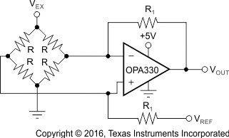 Figure 23. Single Operational Amplifier Bridge Amplifier Schematic
9.3.2 Low-Side Current Monitor
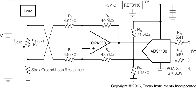
A low-side current shunt monitor is shown in Figure 24.
RN are operational resistors used to isolate the ADS1100 from the noise of the digital I2C bus. Because the ADS1100 is a 16-bit converter, a precise reference is essential for maximum accuracy. If absolute accuracy is not required, and the 5-V power supply is sufficiently stable, the REF3130 may be omitted.
NOINDENT:
NOTE: 1% resistors provide adequate common-mode rejection at small ground-loop errors.9.3.3 Thermistor Measurement
Figure 25 shows the OPA330 in a typical thermistor circuit.
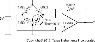 Figure 25. Thermistor Measurement Schematic


