ZHCSF20A May 2016 – May 2016 OPA2377-Q1 , OPA377-Q1 , OPA4377-Q1
PRODUCTION DATA.
6 Specifications
6.1 Absolute Maximum Ratings
over operating free-air temperature range (unless otherwise noted)(1)| MIN | MAX | UNIT | ||
|---|---|---|---|---|
| VS = (V+) – (V–) | Supply voltage | 7 | V | |
| Signal input terminal voltage(2) | (V–) – 0.5 | (V+) + 0.5 | V | |
| Signal input terminal current(2) | –10 | 10 | mA | |
| Output short-circuit current(3) | Continuous | |||
| TA | Operating temperature | –40 | 150 | °C |
| TJ | Junction temperature | 150 | °C | |
| Tstg | Storage temperature | –65 | 150 | °C |
(1) Stresses beyond those listed under Absolute Maximum Ratings may cause permanent damage to the device. These are stress ratings only, which do not imply functional operation of the device at these or any other conditions beyond those indicated under Recommended Operating Conditions. Exposure to absolute-maximum-rated conditions for extended periods may affect device reliability.
(2) Input terminals are diode-clamped to the power-supply rails. Input signals that can swing more than 0.5 V beyond the supply rails should be current limited to 10 mA or less.
(3) Short-circuit to ground, one amplifier per package.
6.2 ESD Ratings
| VALUE | UNIT | |||
|---|---|---|---|---|
| V(ESD) | Electrostatic discharge | Human-body model (HBM), per AEC Q100-002(1) | ±4000 | V |
| Charged-device model (CDM), per AEC Q100-011 | ±1000 | |||
(1) AEC Q100-002 indicates that HBM stressing shall be in accordance with the ANSI/ESDA/JEDEC JS-001 specification.
6.3 Recommended Operating Conditions
over operating free-air temperature range (unless otherwise noted)| MIN | MAX | UNIT | ||
|---|---|---|---|---|
| Supply voltage | 2.2 | 5.5 | V | |
| TA | Operating temperature | –40 | 150 | °C |
6.4 Thermal Information: OPA377-Q1
| THERMAL METRIC(1) | OPA377-Q1 | UNIT | |
|---|---|---|---|
| DBV (SOT23) | |||
| 5 PINS | |||
| RθJA | Junction-to-ambient thermal resistance | 273.8 | °C/W |
| RθJC(top) | Junction-to-case (top) thermal resistance | 126.8 | °C/W |
| RθJB | Junction-to-board thermal resistance | 85.9 | °C/W |
| ψJT | Junction-to-top characterization parameter | 10.9 | °C/W |
| ψJB | Junction-to-board characterization parameter | 84.9 | °C/W |
| RθJC(bot) | Junction-to-case (bottom) thermal resistance | n/a | °C/W |
(1) For more information about traditional and new thermal metrics, see the Semiconductor and IC Package Thermal Metrics application report, SPRA953.
6.5 Thermal Information: OPA2377-Q1
| THERMAL METRIC(1) | OPA2377-Q1 | UNIT | |
|---|---|---|---|
| DGK (VSSOP) | |||
| 8 PINS | |||
| RθJA | Junction-to-ambient thermal resistance | 171.2 | °C/W |
| RθJC(top) | Junction-to-case (top) thermal resistance | 63.9 | °C/W |
| RθJB | Junction-to-board thermal resistance | 92.8 | °C/W |
| ψJT | Junction-to-top characterization parameter | 9.2 | °C/W |
| ψJB | Junction-to-board characterization parameter | 91.2 | °C/W |
| RθJC(bot) | Junction-to-case (bottom) thermal resistance | n/a | °C/W |
(1) For more information about traditional and new thermal metrics, see the Semiconductor and IC Package Thermal Metrics application report, SPRA953.
6.6 Thermal Information: OPA4377-Q1
| THERMAL METRIC(1) | OPA4377-Q1 | UNIT | |
|---|---|---|---|
| PW (TSSOP) | |||
| 14 PINS | |||
| RθJA | Junction-to-ambient thermal resistance | 107.8 | °C/W |
| RθJC(top) | Junction-to-case (top) thermal resistance | 29.6 | °C/W |
| RθJB | Junction-to-board thermal resistance | 52.6 | °C/W |
| ψJT | Junction-to-top characterization parameter | 1.5 | °C/W |
| ψJB | Junction-to-board characterization parameter | 51.6 | °C/W |
| RθJC(bot) | Junction-to-case (bottom) thermal resistance | n/a | °C/W |
(1) For more information about traditional and new thermal metrics, see the Semiconductor and IC Package Thermal Metrics application report, SPRA953.
6.7 Electrical Characteristics: VS = 2.2 V to 5.5 V
At TA = 25°C, RL = 10 kΩ connected to VS/2, VCM = VS/2, and VOUT = VS/2, unless otherwise noted.| PARAMETER | TEST CONDITIONS | MIN | TYP | MAX | UNIT | |
|---|---|---|---|---|---|---|
| OFFSET VOLTAGE | ||||||
| VOS | Input offset voltage | VS = 5 V | 0.25 | 1 | mV | |
| Input offset voltage versus temperature |
At TA = –40°C to +125°C, VS = 2.2 V to 5.5 V, VCM < (V+) – 1.3 V |
5 | µV/V | |||
| dVOS/dT | Input offset voltage versus drift |
At TA = –40°C to +125°C | 0.32 | 2 | μV/°C | |
| PSRR | Input offset voltage versus power supply |
At TA = 25°C, VS = 2.2 V to 5.5 V, VCM < (V+) – 1.3 V |
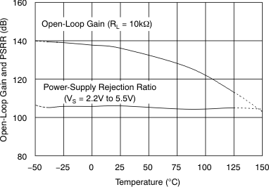
5 | 28 | μV/V | |
| Channel separation, dc (dual, quad) | 0.5 | µV/V | ||||
| INPUT BIAS CURRENT | ||||||
| IIB | Input bias current | ±0.2 | ±10 | pA | ||
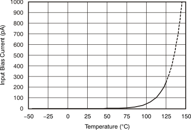
| Input bias current versus temperature |
See Typical Characteristics | pA | ||||
| IOS | Input offset current | ±0.2 | ±10 | pA | ||
| NOISE | ||||||
| Input voltage noise | f = 0.1 Hz to 10 Hz | 0.8 | μVPP | |||
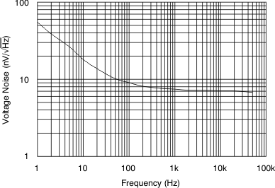
| en | Input voltage noise density | f = 1 kHz | 7.5 | nV/√Hz | ||
| in | Input current noise density | f = 1 kHz | 2 | fA/√Hz | ||
| INPUT VOLTAGE RANGE | ||||||
| VCM | Common-mode voltage range | (V–) – 0.1 | (V+) + 0.1 | V | ||
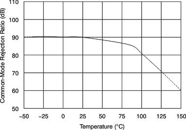
| CMRR | Common-mode rejection ratio | (V–) < VCM < (V+) – 1.3 V | 70 | 90 | dB | |
| INPUT CAPACITANCE | ||||||
| Differential | 6.5 | pF | ||||
| Common-mode | 13 | pF | ||||
| OPEN-LOOP GAIN | ||||||
| AOL | Open-loop voltage gain | 50 mV < VO < (V+) – 50 mV, RL = 10 kΩ | 112 | 134 | dB | |
| 100 mV < VO < (V+) – 100 mV, RL = 2 kΩ | 126 | dB | ||||
| FREQUENCY RESPONSE, VS = 5.5 V | ||||||
| GBW | Gain-bandwidth product | 5.5 | MHz | |||
| SR | Slew rate | G = +1 | 2 | V/μs | ||
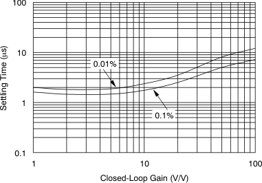
| tS | Settling time | At 0.1%, 2-V step, G = +1 | 1.6 | μs | ||
| At 0.01%, 2-V step, G = +1 | 2 | μs | ||||
| Overload recovery time | VIN × Gain > VS | 0.33 | μs | |||
| THD+N | Total harmonic distortion + noise | VO = 1 VRMS, G = +1, f = 1 kHz, RL = 10 kΩ | 0.00027% | |||
| OUTPUT | ||||||
| Voltage output swing from rail | At TA = 25°C, RL = 10 kΩ | 10 | 20 | mV | ||
| At TA = –40°C to +125°C, RL = 10 kΩ | 40 | mV | ||||
| ISC | Short-circuit current | +30/–50 | mA | |||
| CLOAD | Capacitive load drive | See Typical Characteristics | ||||
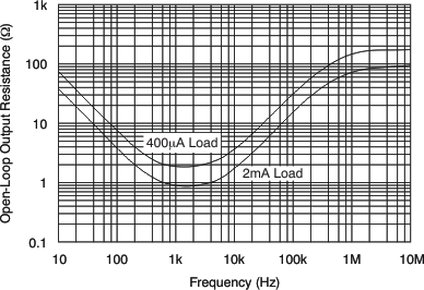
| RO | Open-loop output impedance | 150 | Ω | |||
| POWER SUPPLY | ||||||
| VS | Specified voltage | 2.2 | 5.5 | V | ||
| IQ | Quiescent current (per amplifier) |
At TA = 25°C, IO = 0, VS = 5.5 V | 0.76 | 1.05 | mA | |
| At TA = –40°C to +125°C | 1.2 | mA | ||||
| TEMPERATURE | ||||||
| Specified temperature | –40 | +125 | °C | |||
6.8 Typical Characteristics
At TA = 25°C, VS = 5 V, RL = 10 kΩ connected to VS/2, VCM = VS/2, and VOUT = VS/2, unless otherwise noted.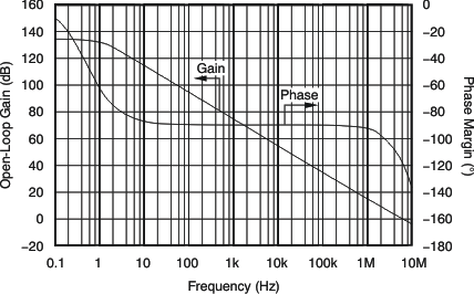
Rejection Ratio vs Temperature
vs Temperature
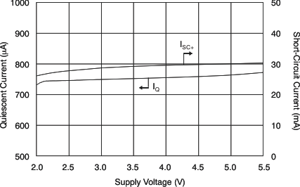
vs Supply Voltage
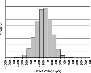
Production Distribution
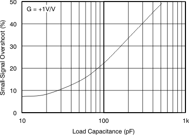
Small-Signal Overshoot vs Load Capacitance
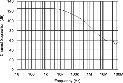
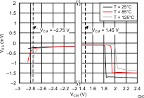
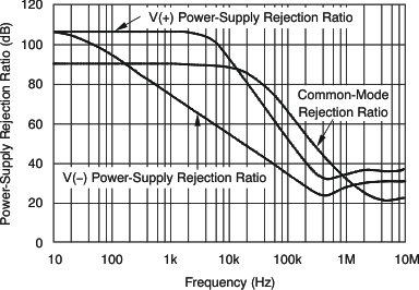
Rejection Ratio vs Frequency
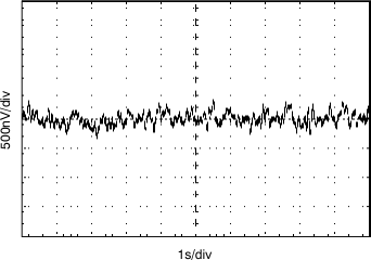
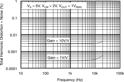
vs Frequency
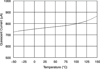
vs Temperature
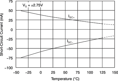
vs Temperature
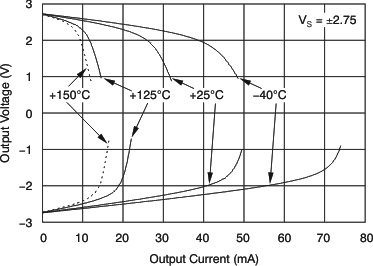
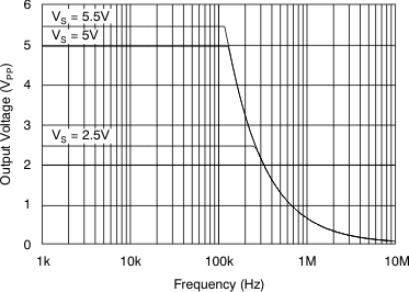
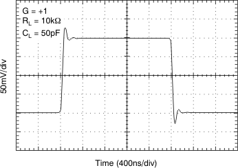
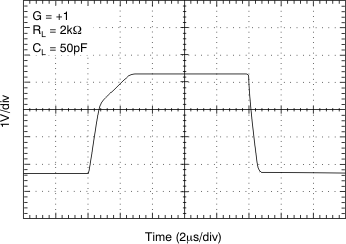
Small-Signal Pulse Response
