ZHCSMO3J june 2020 – june 2023 OPA2863 , OPA4863 , OPA863
PRODUCTION DATA
- 1
- 1 特性
- 2 应用
- 3 说明
- 4 Revision History
- 5 Device Comparison Table
- 6 Pin Configuration and Functions
-
7 Specifications
- 7.1 Absolute Maximum Ratings
- 7.2 ESD Ratings
- 7.3 Recommended Operating Conditions
- 7.4 Thermal Information: OPA863
- 7.5 Thermal Information: OPA2863
- 7.6 Thermal Information: OPA4863
- 7.7 Electrical Characteristics: VS = 10 V
- 7.8 Electrical Characteristics: VS = 3 V
- 7.9 Typical Characteristics: VS = 10 V
- 7.10 Typical Characteristics: VS = 3 V
- 7.11 Typical Characteristics: VS = 3 V to 10 V
- 8 Detailed Description
- 9 Application and Implementation
- 10Device and Documentation Support
- 11Mechanical, Packaging, and Orderable Information
封装选项
机械数据 (封装 | 引脚)
散热焊盘机械数据 (封装 | 引脚)
订购信息
9.2.1.2 Detailed Design Procedure
In a difference amplifier circuit, the output voltage is given by:
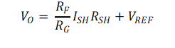
For lowest system noise, small values of RF and RG are preferred. The smallest value of RG is limited by the input transient voltage (10 V here) seen by the circuit, and is given by:
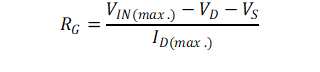
Where,
- VIN(maximum) is the maximum input transient voltage seen by the circuit.
- VD is the forward voltage drop of ESD diodes at the amplifier input.
- ID(maximum) is the maximum current rating of the ESD diodes at the amplifier input.
For a difference amplifier gain of 20 V/V, an RF of 12 kΩ and RG of 600 Ω are used. With a clock frequency of 40 MHz and the ADS7056 sampling at 1 MSPS, the available acquisition time for amplifier output settling is 550 ns. Figure 9-2 shows the simulation results for the circuit in Figure 9-1. The worst-case peak-to-peak input transient condition is simulated. The output of the OPAx863 device settles to within 0.1% accuracy within 543 ns. If using a slower clock frequency with the ADC is desired, then the acquisition time reduces with the same sampling rate, which degrades measurement accuracy. Alternatively, the sampling rate can be reduced to recover the required acquisition time and 0.1% accuracy.