ZHCSI16F March   2002  – April 2018 OPA2357 , OPA357

PRODUCTION DATA.  

  1. 1 特性
  2. 2 应用
  3. 3 说明
    1.     Device Images
      1.      简化原理图
  4. 4 修订历史记录
  5. 5 Pin Configuration and Functions
    1.     Pin Functions
  6. 6 Specifications
    1. 6.1 Absolute Maximum Ratings
    2. 6.2 ESD Ratings
    3. 6.3 Recommended Operating Conditions
    4. 6.4 Thermal Information
    5. 6.5 Electrical Characteristics: VS = +2.7-V to +5.5-V Single-Supply
    6. 6.6 Typical Characteristics
  7. 7 Detailed Description
    1. 7.1 Overview
    2. 7.2 Functional Block Diagram
    3. 7.3 Feature Description
      1. 7.3.1  OPAx357 Comparison
      2. 7.3.2  Operating Voltage
      3. 7.3.3  Enable Function
      4. 7.3.4  Rail-to-Rail Input
      5. 7.3.5  Rail-to-Rail Output
      6. 7.3.6  Output Drive
      7. 7.3.7  Video
      8. 7.3.8  Wideband Video Multiplexing
      9. 7.3.9  Driving Analog-to-Digital Converters
      10. 7.3.10 Capacitive Load and Stability
      11. 7.3.11 Wideband Transimpedance Amplifier
    4. 7.4 Device Functional Modes
  8. 8 Application and Implementation
    1. 8.1 Application Information
    2. 8.2 Typical Applications
      1. 8.2.1 Transimpedance Amplifier
        1. 8.2.1.1 Design Requirements
        2. 8.2.1.2 Detailed Design Procedure
          1. 8.2.1.2.1 Custom Design With WEBENCH® Tools
          2. 8.2.1.2.2 OPAx357 Design Procedure
            1. 8.2.1.2.2.1 Optimizing the Transimpedance Circuit
        3. 8.2.1.3 Application Curve
      2. 8.2.2 High-Impedance Sensor Interface
      3. 8.2.3 Driving ADCs
      4. 8.2.4 Active Filter
  9. 9 Power Supply Recommendations
    1. 9.1 Power Dissipation
  10. 10Layout
    1. 10.1 Layout Guidelines
    2. 10.2 Layout Example
  11. 11器件和文档支持
    1. 11.1 器件支持
      1. 11.1.1 开发支持
        1. 11.1.1.1 使用 WEBENCH® 工具创建定制设计
    2. 11.2 文档支持
      1. 11.2.1 相关文档
    3. 11.3 相关链接
    4. 11.4 接收文档更新通知
    5. 11.5 社区资源
    6. 11.6 商标
    7. 11.7 静电放电警告
    8. 11.8 Glossary
  12. 12机械、封装和可订购信息

封装选项

机械数据 (封装 | 引脚)
散热焊盘机械数据 (封装 | 引脚)
订购信息

Typical Characteristics

at TA = 25°C, VS = 5 V, G = +1, RF = 0 Ω, RL = 1 kΩ, and connected to VS / 2 (unless otherwise noted)
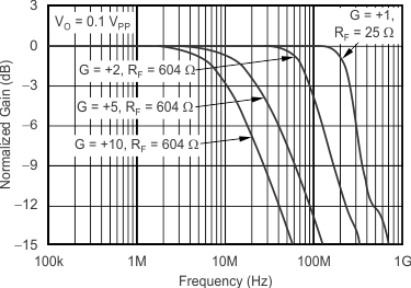
OPA357 OPA2357 OPA357_SBOS235_G001.gif
Figure 1. Noninverting Small-Signal Frequency Response
OPA357 OPA2357 OPA357_SBOS235_G003.gif
Figure 3. Noninverting Small-Signal Step Response
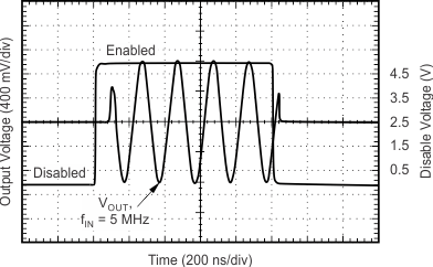
OPA357 OPA2357 OPA357_SBOS235_G005.gif
Figure 5. Large-Signal Disable, Enable Response
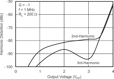
OPA357 OPA2357 OPA357_SBOS235_G007.gif
Figure 7. Harmonic Distortion vs Output Voltage
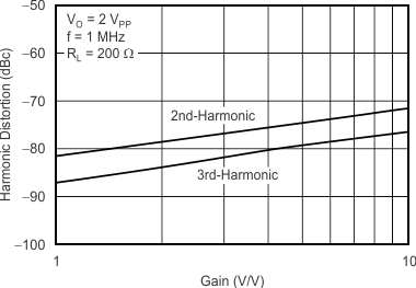
OPA357 OPA2357 OPA357_SBOS235_G009.gif
Figure 9. Harmonic Distortion vs Inverting Gain
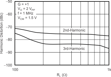
OPA357 OPA2357 OPA357_SBOS235_G011.gif
Figure 11. Harmonic Distortion vs Load Resistance
OPA357 OPA2357 OPA357_SBOS235_G013.gif
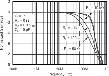
Figure 13. Frequency Response for Various RL
OPA357 OPA2357 OPA357_SBOS235_G015.gif
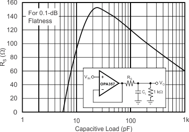
Figure 15. Recommended RS vs Capacitive Load
OPA357 OPA2357 OPA357_SBOS235_G017.gif
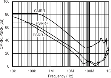
Figure 17. Common-Mode Rejection Ratio and Power-Supply Rejection Ratio vs Frequency
OPA357 OPA2357 OPA357_SBOS235_G019.gif
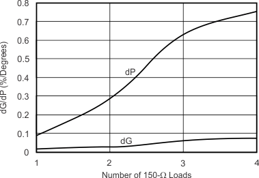
Figure 19. Composite Video differential Gain and Phase
OPA357 OPA2357 OPA357_SBOS235_G021.gif
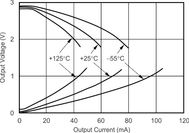
VS = 3 V
Figure 21. Output Voltage Swing vs Output Current
OPA357 OPA2357 OPA357_SBOS235_G023.gif
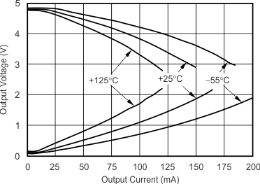
VS = 5 V
Figure 23. Output Voltage Swing vs Output Current
OPA357 OPA2357 OPA357_SBOS235_G025.gif
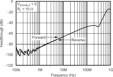
Figure 25. Disable Feedthrough vs Frequency
OPA357 OPA2357 OPA357_SBOS235_G027.gif
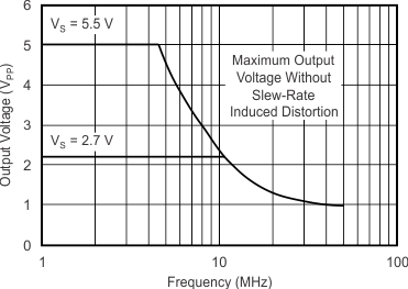
Figure 27. Maximum Output Voltage vs Frequency
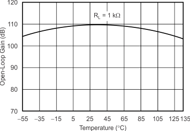
OPA357 OPA2357 OPA357_SBOS235_G029.gif
Figure 29. Open-Loop Gain vs Temperature
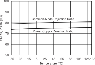
OPA357 OPA2357 OPA357_SBOS235_G031.gif
Figure 31. Common-Mode Rejection Ratio and Power-Supply Rejection Ratio vs Temperature
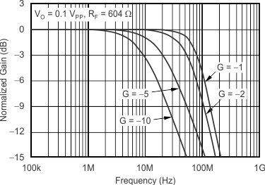
OPA357 OPA2357 OPA357_SBOS235_G002.gif
Figure 2. Inverting Small-Signal Frequency Response
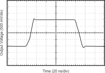
OPA357 OPA2357 OPA357_SBOS235_G004.gif
Figure 4. Noninverting Large-Signal Step Response
OPA357 OPA2357 OPA357_SBOS235_G006.gif
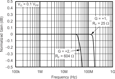
Figure 6. 0.1-dB Gain Flatness
OPA357 OPA2357 OPA357_SBOS235_G008.gif
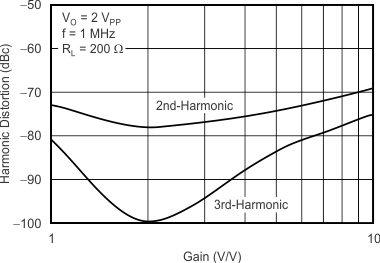
Figure 8. Harmonic Distortion vs Noninverting Gain
OPA357 OPA2357 OPA357_SBOS235_G010.gif
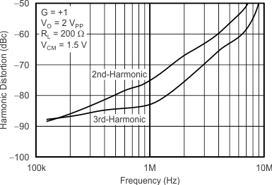
Figure 10. Harmonic Distortion vs Frequency
OPA357 OPA2357 OPA357_SBOS235_G012.gif
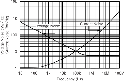
Figure 12. Input Voltage and Current Noise Spectral Density vs Frequency
OPA357 OPA2357 OPA357_SBOS235_G014.gif
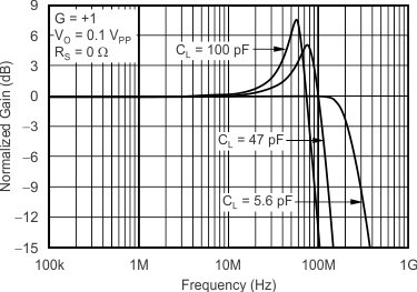
Figure 14. Frequency Response for Various CL
OPA357 OPA2357 OPA357_SBOS235_G016.gif
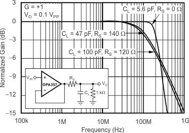
Figure 16. Frequency Response vs Capacitive Load
OPA357 OPA2357 OPA357_SBOS235_G018.gif
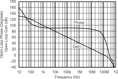
Figure 18. Open-Loop Gain and Phase
OPA357 OPA2357 OPA357_SBOS235_G020.gif
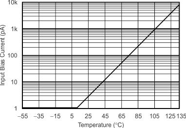
Figure 20. Input Bias Current vs Temperature
OPA357 OPA2357 OPA357_SBOS235_G022.gif
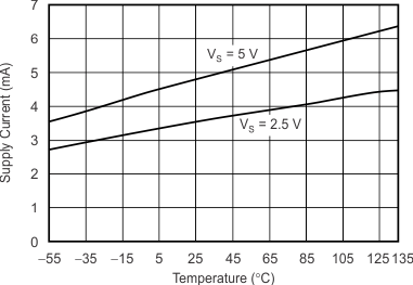
Figure 22. Supply Current vs Temperature
OPA357 OPA2357 OPA357_SBOS235_G024.gif
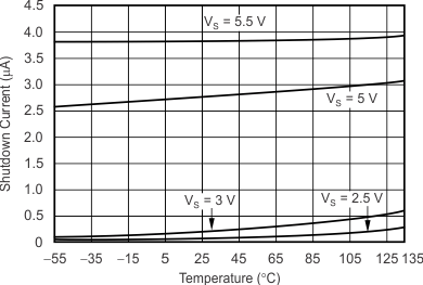
Figure 24. Shutdown Current vs Temperature
OPA357 OPA2357 OPA357_SBOS235_G026.gif
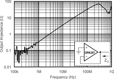
Figure 26. Closed-Loop Output Impedance vs Frequency
OPA357 OPA2357 OPA357_SBOS235_G028.gif
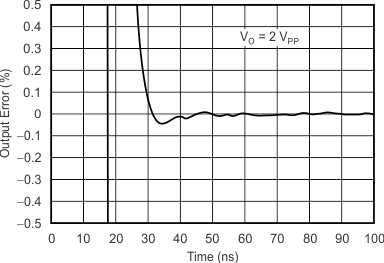
Figure 28. Output Settling Time to 0.1%
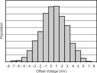
OPA357 OPA2357 OPA357_SBOS235_G030.gif
Figure 30. Offset Voltage Production Distribution
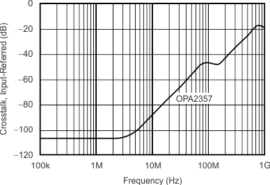
OPA357 OPA2357 OPA357_SBOS235_G032.gif
Figure 32. Channel-to-Channel Crosstalk