ZHCSEE5B November 2015 – May 2016 OPA1622
PRODUCTION DATA.
8 Application and Implementation
NOTE
Information in the following applications sections is not part of the TI component specification, and TI does not warrant its accuracy or completeness. TI’s customers are responsible for determining suitability of components for their purposes. Customers should validate and test their design implementation to confirm system functionality.
8.1 Application Information
The low noise and distortion of the OPA1622 make the device well suited for a variety of applications in professional and consumer audio products. However, these same performance metrics also make the OPA1622 useful for industrial, test-and-measurement, and data-acquisition applications. The example shown here is only one possible application where the OPA1622 provides exceptional performance.
8.1.1 Noise Performance
Figure 49 shows the total circuit noise for varying source impedances with the op amp in a unity-gain configuration (no feedback resistor network, and therefore no additional noise contributions).
The OPA1622 is shown with total circuit noise calculated. The op amp contributes both a voltage noise component and a current noise component. The voltage noise is commonly modeled as a time-varying component of the offset voltage. The current noise is modeled as the time-varying component of the input bias current, and reacts with the source resistance to create a voltage component of noise. Therefore, the lowest noise op amp for a given application depends on the source impedance. For low source impedance, current noise is negligible, and voltage noise generally dominates. The low voltage and current noise of the OPA1622 op amp make the device an excellent choice for use in applications where the source impedance is less than 10 kΩ.
8.1.1.1 Noise Calculations
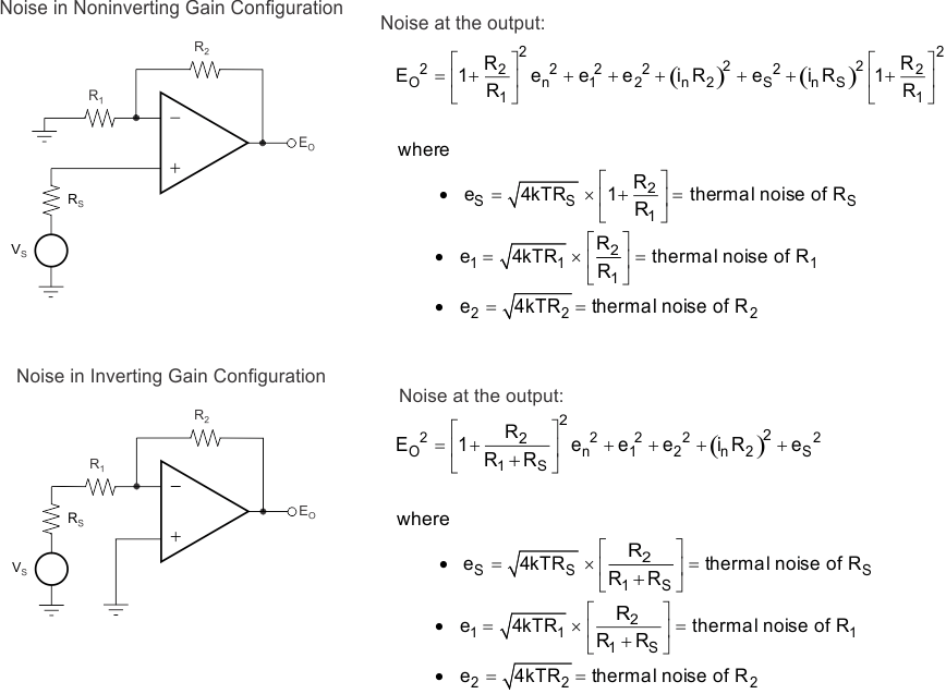
The equations in Figure 50 show the calculation of the total circuit noise using these parameters:
- en = voltage noise
- In = current noise
- RS = source impedance
- k = Boltzmann’s constant = 1.38 × 10⁻²³ J/K
- T = temperature in kelvins (K)
8.1.1.2 Application Curve
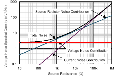 Figure 49. Noise Performance of the OPA1622 in a Unity-Gain Buffer Configuration
8.1.1.3 Basic Noise Calculations
Designing low-noise op amp circuits requires careful consideration of a variety of possible noise contributors, such as noise from the signal source, noise generated in the op amp, and noise from the feedback network resistors. The total noise of the circuit is the root sum squared combination of all noise components.
The resistive portion of the source impedance produces thermal noise proportional to the square root of the resistance. Figure 49 plots this function. The source impedance is usually fixed; consequently, select the op amp and the feedback resistors to minimize the respective contributions to the total noise.
Figure 50 shows both inverting and noninverting op amp circuit configurations with gain. In circuit configurations with gain, the feedback network resistors also contribute noise.
The current noise of the op amp reacts with the feedback resistors to create additional noise components. Choose feedback resistor values that make these noise sources negligible. The equations for total noise are shown for both configurations.
NOINDENT:
For the OPA1622 at 1 kHz, en = 2.8 nV/√Hz and in = 800 fA/√Hz.8.1.2 Total Harmonic Distortion Measurements
The distortion produced by OPA1622 is below the measurement limit of many commercially-available distortion analyzers. However, a special test circuit, as shown in Figure 51, can be used to extend the measurement capabilities.
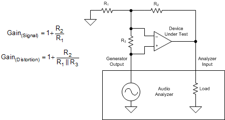 Figure 51. Distortion Test Circuit
Consider op amp distortion an internal error source that is referred to the input. Figure 51 shows a circuit that causes the op amp distortion to be 101 times (approximately 40 dB) greater than that normally produced by the op amp. The addition of R3 to the otherwise standard noninverting amplifier configuration alters the feedback factor or noise gain of the circuit. The closed-loop gain is unchanged, but the feedback available for error correction is reduced by a factor of 101, thus extending the resolution by 101. Note that the input signal and load applied to the op amp are the same as with conventional feedback without R3. Keep the value of R3 small to minimize its effect on the distortion measurements.
Verify the validity of this technique by duplicating measurements at high gain or high frequency where the distortion is within the measurement capability of the test equipment.
8.2 Typical Application
The low distortion and high output-current capabilities of the OPA1622 make this device an excellent choice for headphone-amplifier applications in portable or studio applications. These applications typically employ an audio digital-to-analog converter (DAC) and a separate headphone amplifier circuit connected to the DAC output. High-performance audio DACs can have an output signal that is either a varying current or voltage. Voltage output configurations require less external circuitry, and therefore have advantages in cost, power consumption, and solution size. However, these configurations can offer slightly lower performance than current output configurations. Differential outputs are standard on both types of DACs. Differential outputs double the output signal levels that can be delivered on a single, low-voltage supply, and also allow for even-harmonics common to both outputs to be cancelled by external circuitry. A simplified representation of a voltage-output audio DAC is shown in Figure 52. Two ac voltage sources (VAC) deliver the output signal to the complementary outputs through their associated output impedances (ROUT). Both output signals have a dc component as well, represented by dc voltage source VDC. The headphone amplifier circuit connected to the output of an audio DAC must convert the differential output into a single-ended signal and be capable of producing signals of sufficient amplitude at the headphones to achieve reasonable listening levels.
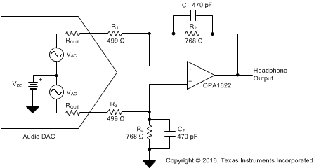 Figure 52. OPA1622 Used as a Headphone Amplifier for a Voltage-Output Audio DAC
8.2.1 Design Requirements
- ±5-V power supplies
- 150-mW output power (32-Ω load)
- < –115-dB THD+N at maximum output (32-Ω load)
- < 0.01-dB magnitude deviation (20 Hz to 20 kHz)
8.2.2 Detailed Design Procedure
Figure 52 shows a schematic of a headphone amplifier circuit for voltage output DACs. An op amp is configured as a difference amplifier that converts the differential output voltage to single-ended. The values of the resistors in the difference amplifier circuit are determined by the specifications of the DAC, such as output voltage and output impedance, as well as the maximum output voltage desired at the headphone output. The op amp chosen must be capable of delivering the necessary current to the headphones and remain stable into typical headphone loads that can have capacitances as high as 400 pF. The following design process uses a hypothetical DAC with common values of output voltage and impedance for the design process. The specifications of the DAC are shown in Table 1:
Table 1. Audio DAC Specifications Used for the Design Process
| PARAMETER | VALUE |
|---|---|
| Maximum differential output voltage | 2 VRMS |
| Output impedance (ROUT) | 200 Ω |
| Output dc offset | 1.65 V |
The gain of the difference amplifier in Figure 52 is determined by the resistor values, and includes the output impedance of the DAC. For R2 = R4 and R1 = R3, the output voltage of the headphone amplifier circuit is shown in Equation 5:

The output voltage required for headphones depends on the headphone impedance, as well as the headphone efficiency (η), a measure of the sound pressure level (SPL, measured in dB) for a certain input power level (typically given at 1 mW). The headphone SPL at other power levels is calculated using Equation 6:

where
- η = efficiency
- PIN = input power to the headphones
Figure 53 shows the input power required to produce certain SPLs for different headphone efficiencies. Typically, over-the-ear style headphones have lower efficiencies than in-ear types with 95 dB/mW being a common value.
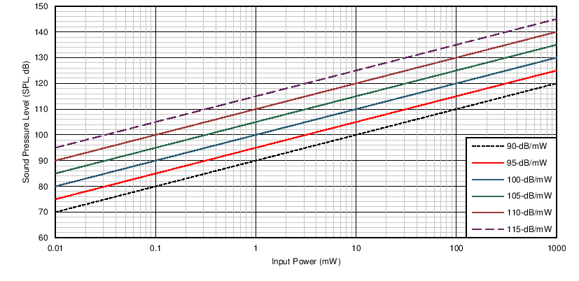 Figure 53. Sound Pressure Level vs Input Power for Headphones of Various Efficiencies
In-ear headphones can have efficiencies of 115 dB/mW or greater, and therefore have much lower power requirements. The output power goal for this design is 150 mW; sufficient power to produce extremely loud sound pressure levels in a wide range of headphones. A 32-Ω headphone impedance is used for this requirement because 32 Ω is a very common value in headphones for portable applications. Equation 7 shows the voltage required for 32-Ω headphones:

A tradeoff exists when selecting resistor values for this design. First, high resistor values contribute additional noise to the circuit, degrading the audio performance. However, extremely low resistor values draw excessive current from the DAC, increasing distortion. A value of 499 Ω is used for resistors R1 and R3 as a reasonable compromise between these two considerations. Resistor R2 and R4 can then be calculated as shown in Equation 8:

In order to accommodate higher impedance headphones, increase the gain of the circuit to produce greater output voltages. However, increasing the gain also increases the noise of the circuit and limits the dynamic range of the circuit into lower impedance headphones. For this reason, some designers choose to select the headphone amplifier gain by using a switch.
Capacitors C1 and C2 limit the bandwidth of the circuit to prevent the unnecessary amplification of interfering signals. The maximum value of these capacitors is determined by the limitations on frequency response magnitude deviation detailed in the Design Requirements section. C1 and C2 combine with resistors R2 and R4 to form a pole, as shown in Equation 9:

Calculate the minimum pole frequency allowable to meet the magnitude deviation requirements using Equation 10:

where
- G represents the gain in decimal for a –0.01-dB deviation at 20 kHz.
Use Equation 11 to calculate the upper limit for the value of C1 and C2 in order to meet the goal for minimal magnitude deviation at 20 kHz.

8.2.3 Application Curves
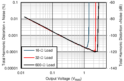
The circuit described in Figure 52 is constructed using 0.1% tolerance thin-film resistors (0603 package) and surface-mount film capacitors. The performance of the circuit is measured using a high-performance audio analyzer and is displayed in Figure 54 through Figure 59. The maximum output power for three common headphone impedances is shown in Table 2
Table 2. Maximum Output Power and THD+N Before Clipping for Common Headphone Impedances
| LOAD IMPEDANCE (Ω) |
MAXIMUM OUTPUT POWER BEFORE CLIPPING (mW) |
THD+N AT MAXIMUM OUTPUT POWER (dB) |
|---|---|---|
| 16 | 95 | –114.2 |
| 32 | 150 | –118.7 |
| 600 | 11.3 | –119.4 |
The maximum output power delivered to low impedance headphone loads (16 Ω and 32 Ω) is limited by the output current capabilities of the amplifier. For the 600-Ω case, the maximum power delivered is limited by the output voltage capability of the amplifier and depends greatly on the power-supply voltages used. Figure 55 shows the maximum output voltage achievable for each load before the onset of clipping (±5-V supplies), indicated by a sharp increase in distortion.
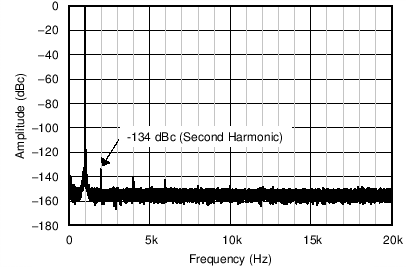
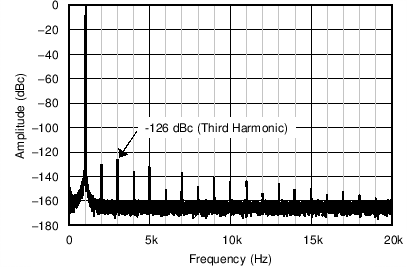
As more current is delivered by the output transistors of an amplifier, additional distortion is produced. At low frequencies, this distortion is corrected by the feedback loop of the amplifier. However, as the loop gain of the amplifier begins to decline at high frequencies, the overall distortion begins to climb. The unique output stage design of the OPA1622 greatly reduces the additional distortion at high frequency when delivering large currents, as shown in Figure 56. High-ordered harmonics (above the 2nd and 3rd) are also kept to a minimal level at high output powers, as shown in Figure 57 through Figure 59.
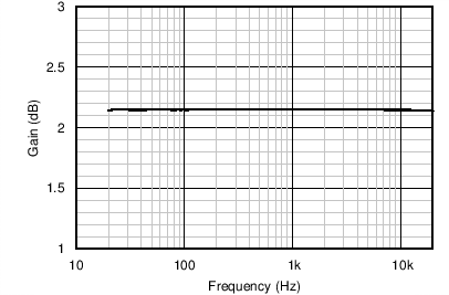
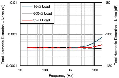
| 90-kHz measurement bandwidth, 1-VRMS output |
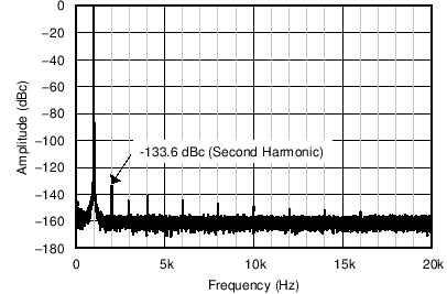
| 1 kHz, 32-Ω load, 50 mW |
| 22.4-kHz measurement bandwidth |
| 1 kHz, 32-Ω load, 10 mW |
| 1 kHz, 32-Ω load, 150 mW |