ZHCSF95C December 2015 – February 2018 LMR23610
PRODUCTION DATA.
- 1 特性
- 2 应用
- 3 说明
- 4 修订历史记录
- 5 Pin Configuration and Functions
- 6 Specifications
-
7 Detailed Description
- 7.1 Overview
- 7.2 Functional Block Diagram
- 7.3
Feature Description
- 7.3.1 Fixed Frequency Peak Current Mode Control
- 7.3.2 Adjustable Output Voltage
- 7.3.3 EN/SYNC
- 7.3.4 VCC, UVLO
- 7.3.5 Minimum ON-Time, Minimum OFF-Time and Frequency Foldback at Dropout Conditions
- 7.3.6 Internal Compensation and CFF
- 7.3.7 Bootstrap Voltage (BOOT)
- 7.3.8 Overcurrent and Short-Circuit Protection
- 7.3.9 Thermal Shutdown
- 7.4 Device Functional Modes
-
8 Application and Implementation
- 8.1 Application Information
- 8.2
Typical Applications
- 8.2.1 Design Requirements
- 8.2.2
Detailed Design Procedure
- 8.2.2.1 Custom Design With WEBENCH® Tools
- 8.2.2.2 Output Voltage Setpoint
- 8.2.2.3 Switching Frequency
- 8.2.2.4 Inductor Selection
- 8.2.2.5 Output Capacitor Selection
- 8.2.2.6 Feed-Forward Capacitor
- 8.2.2.7 Input Capacitor Selection
- 8.2.2.8 Bootstrap Capacitor Selection
- 8.2.2.9 VCC Capacitor Selection
- 8.2.2.10 Undervoltage Lockout Setpoint
- 8.2.3 Application Curves
- 9 Power Supply Recommendations
- 10Layout
- 11器件和文档支持
- 12机械、封装和可订购信息
7.3.3 EN/SYNC
The voltage on the EN pin controls the ON or OFF operation of LMR23610. A voltage less than 1 V (typical) shuts down the device while a voltage higher than 1.6 V (typical) is required to start the regulator. The EN pin is an input and can not be left open or floating. The simplest way to enable the operation of the LMR23610 is to connect the EN to VIN. This allows self-start-up of the LMR23610 when VIN is within the operation range.
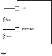
Many applications will benefit from the employment of an enable divider RENT and RENB (Figure 15) to establish a precision system UVLO level for the converter. System UVLO can be used for supplies operating from utility power as well as battery power. It can be used for sequencing, ensuring reliable operation, or supply protection, such as a battery discharge level. An external logic signal can also be used to drive EN input for system sequencing and protection.
 Figure 15. System UVLO by Enable Divider
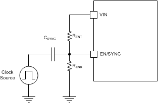
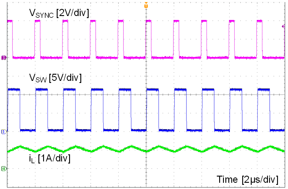
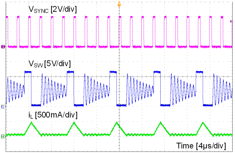
The EN pin also can be used to synchronize the internal oscillator to an external clock. The internal oscillator can be synchronized by AC coupling a positive edge into the EN pin. The AC coupled peak-to-peak voltage at the EN pin must exceed the SYNC amplitude threshold of 2.8 V (typical) to trip the internal synchronization pulse detector, and the minimum SYNC clock ON and OFF time must be longer than 100ns (typical). A 3.3 V or a higher amplitude pulse signal coupled through a 1 nF capacitor CSYNC is a good starting point. Keeping RENT // RENB (RENT parallel with RENB) in the 100 kΩ range is a good choice. RENT is required for this synchronization circuit, but RENB can be left unmounted if system UVLO is not needed. LMR23610 switching action can be synchronized to an external clock from 200 kHz to 2.2 MHz. Figure 17 and Figure 18 show the device synchronized to an external system clock.
 Figure 16. Synchronize to external clock
 Figure 17. Synchronizing in PWM Mode
 Figure 18. Synchronizing in PFM Mode