SNAS605AS March 2013 – May 2020 LMK04821 , LMK04826 , LMK04828
PRODUCTION DATA.
- 1 Features
- 2 Applications
- 3 Description
- 4 Revision History
- 5 Device Comparison Table
- 6 Pin Configuration and Functions
- 7 Specifications
- 8 Parameter Measurement Information
-
9 Detailed Description
- 9.1
Overview
- 9.1.1 Jitter Cleaning
- 9.1.2 JEDEC JESD204B Support
- 9.1.3 Three PLL1 Redundant Reference Inputs
- 9.1.4 VCXO/Crystal Buffered Output
- 9.1.5 Frequency Holdover
- 9.1.6 PLL2 Integrated Loop Filter Poles
- 9.1.7 Internal VCOs
- 9.1.8 External VCO Mode
- 9.1.9 Clock Distribution
- 9.1.10 Zero-Delay
- 9.1.11 Status Pins
- 9.2 Functional Block Diagram
- 9.3 Feature Description
- 9.4 Device Functional Modes
- 9.5 Programming
- 9.6 Register Maps
- 9.7
Device Register Descriptions
- 9.7.1 System Functions
- 9.7.2
(0x100 - 0x138) Device Clock and SYSREF Clock Output Controls
- 9.7.2.1 CLKoutX_Y_ODL, CLKoutX_Y_IDL, DCLKoutX_DIV
- 9.7.2.2 DCLKoutX_DDLY_CNTH, DCLKoutX_DDLY_CNTL
- 9.7.2.3 DCLKoutX_ADLY, DCLKoutX_ADLY_MUX, DCLKout_MUX
- 9.7.2.4 DCLKoutX_HS, SDCLKoutY_MUX, SDCLKoutY_DDLY, SDCLKoutY_HS
- 9.7.2.5 SDCLKoutY_ADLY_EN, SDCLKoutY_ADLY
- 9.7.2.6 DCLKoutX_DDLY_PD, DCLKoutX_HSg_PD, DCLKout_ADLYg_PD, DCLKout_ADLY_PD, DCLKoutX_Y_PD, SDCLKoutY_DIS_MODE, SDCLKoutY_PD
- 9.7.2.7 SDCLKoutY_POL, SDCLKoutY_FMT, DCLKoutX_POL, DCLKoutX_FMT
- 9.7.3
SYSREF, SYNC, and Device Config
- 9.7.3.1 VCO_MUX, OSCout_MUX, OSCout_FMT
- 9.7.3.2 SYSREF_CLKin0_MUX, SYSREF_MUX
- 9.7.3.3 SYSREF_DIV[12:8], SYSREF_DIV[7:0]
- 9.7.3.4 SYSREF_DDLY[12:8], SYSREF_DDLY[7:0]
- 9.7.3.5 SYSREF_PULSE_CNT
- 9.7.3.6 PLL2_NCLK_MUX, PLL1_NCLK_MUX, FB_MUX, FB_MUX_EN
- 9.7.3.7 PLL1_PD, VCO_LDO_PD, VCO_PD, OSCin_PD, SYSREF_GBL_PD, SYSREF_PD, SYSREF_DDLY_PD, SYSREF_PLSR_PD
- 9.7.3.8 DDLYdSYSREF_EN, DDLYdX_EN
- 9.7.3.9 DDLYd_STEP_CNT
- 9.7.3.10 SYSREF_CLR, SYNC_1SHOT_EN, SYNC_POL, SYNC_EN, SYNC_PLL2_DLD, SYNC_PLL1_DLD, SYNC_MODE
- 9.7.3.11 SYNC_DISSYSREF, SYNC_DISX
- 9.7.3.12 Fixed Registers (0x145, 0x171 - 0x172)
- 9.7.4 (0x146 - 0x149) CLKin Control
- 9.7.5 RESET_MUX, RESET_TYPE
- 9.7.6
(0x14B - 0x152) Holdover
- 9.7.6.1 LOS_TIMEOUT, LOS_EN, TRACK_EN, HOLDOVER_FORCE, MAN_DAC_EN, MAN_DAC[9:8]
- 9.7.6.2 MAN_DAC[9:8], MAN_DAC[7:0]
- 9.7.6.3 DAC_TRIP_LOW
- 9.7.6.4 DAC_CLK_MULT, DAC_TRIP_HIGH
- 9.7.6.5 DAC_CLK_CNTR
- 9.7.6.6 CLKin_OVERRIDE, HOLDOVER_PLL1_DET, HOLDOVER_LOS_DET, HOLDOVER_VTUNE_DET, HOLDOVER_HITLESS_SWITCH, HOLDOVER_EN
- 9.7.6.7 HOLDOVER_DLD_CNT[13:8], HOLDOVER_DLD_CNT[7:0]
- 9.7.7
(0x153 - 0x15F) PLL1 Configuration
- 9.7.7.1 CLKin0_R[13:8], CLKin0_R[7:0]
- 9.7.7.2 CLKin1_R[13:8], CLKin1_R[7:0]
- 9.7.7.3 CLKin2_R[13:8], CLKin2_R[7:0]
- 9.7.7.4 PLL1_N
- 9.7.7.5 PLL1_WND_SIZE, PLL1_CP_TRI, PLL1_CP_POL, PLL1_CP_GAIN
- 9.7.7.6 PLL1_DLD_CNT[13:8], PLL1_DLD_CNT[7:0]
- 9.7.7.7 PLL1_R_DLY, PLL1_N_DLY
- 9.7.7.8 PLL1_LD_MUX, PLL1_LD_TYPE
- 9.7.8
(0x160 - 0x16E) PLL2 Configuration
- 9.7.8.1 PLL2_R[11:8], PLL2_R[7:0]
- 9.7.8.2 PLL2_P, OSCin_FREQ, PLL2_XTAL_EN, PLL2_REF_2X_EN
- 9.7.8.3 PLL2_N_CAL
- 9.7.8.4 PLL2_FCAL_DIS, PLL2_N
- 9.7.8.5 PLL2_WND_SIZE, PLL2_CP_GAIN, PLL2_CP_POL, PLL2_CP_TRI
- 9.7.8.6 SYSREF_REQ_EN, PLL2_DLD_CNT
- 9.7.8.7 PLL2_LF_R4, PLL2_LF_R3
- 9.7.8.8 PLL2_LF_C4, PLL2_LF_C3
- 9.7.8.9 PLL2_LD_MUX, PLL2_LD_TYPE
- 9.7.9
(0x16F - 0x1FFF) Misc Registers
- 9.7.9.1 PLL2_PRE_PD, PLL2_PD
- 9.7.9.2 VCO1_DIV
- 9.7.9.3 OPT_REG_1
- 9.7.9.4 OPT_REG_2
- 9.7.9.5 RB_PLL1_LD_LOST, RB_PLL1_LD, CLR_PLL1_LD_LOST
- 9.7.9.6 RB_PLL2_LD_LOST, RB_PLL2_LD, CLR_PLL2_LD_LOST
- 9.7.9.7 RB_DAC_VALUE(MSB), RB_CLKinX_SEL, RB_CLKinX_LOS
- 9.7.9.8 RB_DAC_VALUE
- 9.7.9.9 RB_HOLDOVER
- 9.7.9.10 SPI_LOCK
- 9.1
Overview
- 10Applications and Implementation
- 11Power Supply Recommendations
- 12Layout
- 13Device and Documentation Support
- 14Mechanical, Packaging, and Orderable Information
封装选项
机械数据 (封装 | 引脚)
- NKD|64
散热焊盘机械数据 (封装 | 引脚)
- NKD|64
订购信息
8.2 Differential Voltage Measurement Terminology
The differential voltage of a differential signal can be described by two different definitions, which can cause confusion when reading data sheets or communicating with other engineers. This section addresses the measurement and description of a differential signal, so that the reader can understand and distinguish between the two different definitions.
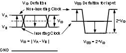
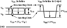
The first definition used to describe a differential signal is the absolute value of the voltage potential between the inverting and non-inverting signal. The symbol for this first measurement is typically VID or VOD, depending on if an input or output voltage is being described.
The second definition used to describe a differential signal is to measure the potential of the non-inverting signal with respect to the inverting signal. The symbol for this second measurement is VSS, and is a calculated parameter. This signal does not exist in the IC with respect to ground; it only exists in reference to its differential pair. VSS can be measured directly by oscilloscopes with floating references; otherwise this value can be calculated as twice the value of VOD, as described in the first description.
Figure 8 illustrates the two different definitions side-by-side for inputs, and Figure 9 illustrates the two different definitions side-by-side for outputs. The VID and VOD definitions show VA and VB DC levels that the non-inverting and inverting signals toggle between with respect to ground. VSS input and output definitions show that if the inverting signal is considered the voltage potential reference, the non-inverting signal voltage potential is now increasing and decreasing above and below the non-inverting reference. Thus, the peak-to-peak voltage of the differential signal can be measured.
VID and VOD are often defined as volts (V) and VSS is often defined as volts peak-to-peak (VPP).
 Figure 8. Two Different Definitions for
Differential Input Signals
 Figure 9. Two Different Definitions for
Differential Output Signals
Refer to application note AN-912 Common Data Transmission Parameters and their Definitions (SNLA036) for more information.