SNOSBY1C June 1999 – December 2015 LMC567
PRODUCTION DATA.
- 1 Features
- 2 Applications
- 3 Description
- 4 Revision History
- 5 Device Comparison Table
- 6 Pin Configuration and Functions
- 7 Specifications
- 8 Parameter Measurement Information
- 9 Detailed Description
- 10Application and Implementation
- 11Power Supply Recommendations
- 12Layout
- 13Device and Documentation Support
- 14Mechanical, Packaging, and Orderable Information
7 Specifications
7.1 Absolute Maximum Ratings
over operating free-air temperature range (unless otherwise noted)(1)(2)| MIN | MAX | UNIT | |||
|---|---|---|---|---|---|
| Input voltage | IN | 2 | Vp–p | ||
| Supply voltage | VCC | 10 | V | ||
| Output voltage | OUT | 13 | V | ||
| Output current | OUT | 30 | mA | ||
| Package dissipation | 500 | mW | |||
| Operating temperature, TA | –25 | 125 | °C | ||
| Storage temperature, Tstg | –55 | 150 | °C | ||
(1) Stresses beyond those listed under Absolute Maximum Ratings may cause permanent damage to the device. These are stress ratings only, which do not imply functional operation of the device at these or any other conditions beyond those indicated under Recommended Operating Conditions. Exposure to absolute-maximum-rated conditions for extended periods may affect device reliability.
(2) If Military/Aerospace specified devices are required, please contact the Texas Instruments Sales Office/Distributors for availability and specifications.
7.2 Recommended Operating Conditions
over operating free-air temperature range (unless otherwise noted)| MIN | MAX | UNIT | ||
|---|---|---|---|---|
| VCC | Supply voltage | 2 | 9 | V |
| FIN | Input frequency | 1 | 500 | Hz |
| TA | Operating temperature | –25 | 125 | °C |
7.3 Thermal Information
| THERMAL METRIC(1) | LMC567 | UNIT | ||
|---|---|---|---|---|
| D (SOIC) | ||||
| 8 PINS | ||||
| RθJA | Junction-to-ambient thermal resistance | 111.8 | °C/W | |
| RθJC(top) | Junction-to-case (top) thermal resistance | 59.2 | °C/W | |
| RθJB | Junction-to-board thermal resistance | 52.2 | °C/W | |
| ψJT | Junction-to-top characterization parameter | 13.5 | °C/W | |
| ψJB | Junction-to-board characterization parameter | 51.7 | °C/W | |
(1) For more information about traditional and new thermal metrics, see the Semiconductor and IC Package Thermal Metrics application report, SPRA953.
7.4 Electrical Characteristics
Test Circuit, TA = 25°C, Vs = 5 V, RtCt #2, Sw. 1 Pos. 0, and no input, unless otherwise noted.| PARAMETER | TEST CONDITIONS | MIN | TYP | MAX | UNIT | ||
|---|---|---|---|---|---|---|---|
| I4 | Power supply current | RtCt #1, quiescent or activated |
Vs = 2 V | 0.3 | mAdc | ||
| Vs = 5 V | 0.5 | 0.8 | |||||
| Vs = 9 V | 0.8 | 1.3 | |||||
| V3 | Input D.C. bias | 0 | mVdc | ||||
| R3 | Input resistance | 40 | kΩ | ||||
| I8 | Output leakage | 1 | 100 | nAdc | |||
| f0 | Center frequency, Fosc ÷ 2 |
RtCt #2, measure oscillator Frequency and divide by 2 |
Vs = 2 V | 98 | kHz | ||
| Vs = 5 V | 92 | 103 | 113 | ||||
| Vs = V | 105 | ||||||
| Δf0 | Center frequency shift with supply |
Equation 1.
 |
1 | 2 | %/V | ||
| Vin | Input threshold | Set input frequency equal to f0 measured above. Increase input level until pin 8 goes low. | Vs = 2 V | 11 | 20 | 27 | mVrms |
| Vs = 5 V | 17 | 30 | 45 | ||||
| Vs = 9 V | 45 | ||||||
| ΔVin | Input hysteresis | Starting at input threshold, decrease input level until pin 8 goes high. |
1.5 | mVrms | |||
| V8 | Output sat voltage | Input level > threshold Choose RL for specified I8. |
I8 = 2 mA | 0.06 | 0.15 | Vdc | |
| I8 = 20 mA | 0.7 | ||||||
| L.D.B.W. | Largest detection bandwidth |
Measure Fosc with Sw. 1 in Pos. 0, 1, and 2; Equation 2.
 |
Vs = 2 V | 7% | 11% | 15% | |
| Vs = 5 V | 11% | 14% | 17% | ||||
| Vs = 9 V | 15% | ||||||
| ΔBW | Bandwidth skew |
Equation 3.
 |
0% | ±1.0% | |||
| fmax | Highest center frequency | RtCt #3 Measure oscillator frequency and divide by 2. |
700 | kHz | |||
| Vin | Input threshold at fmax | Set input frequency equal to fmax measured above. Increase input level until pin 8 goes low. | 35 | mVrms | |||
7.5 Typical Characteristics
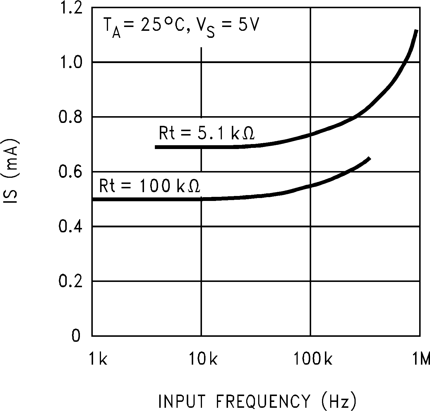 Figure 1. Supply Current vs Operating Frequency
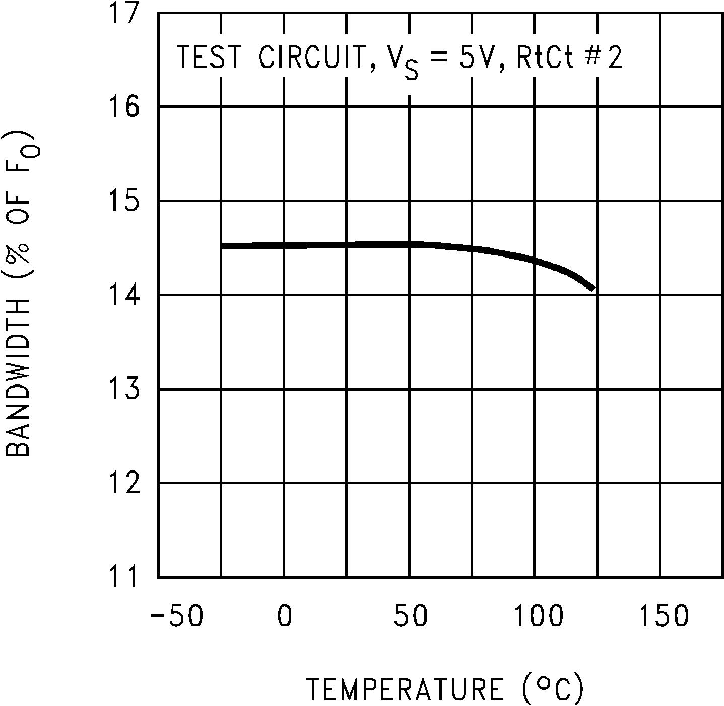 Figure 3. Largest Detection Bandwidth vs Temperature
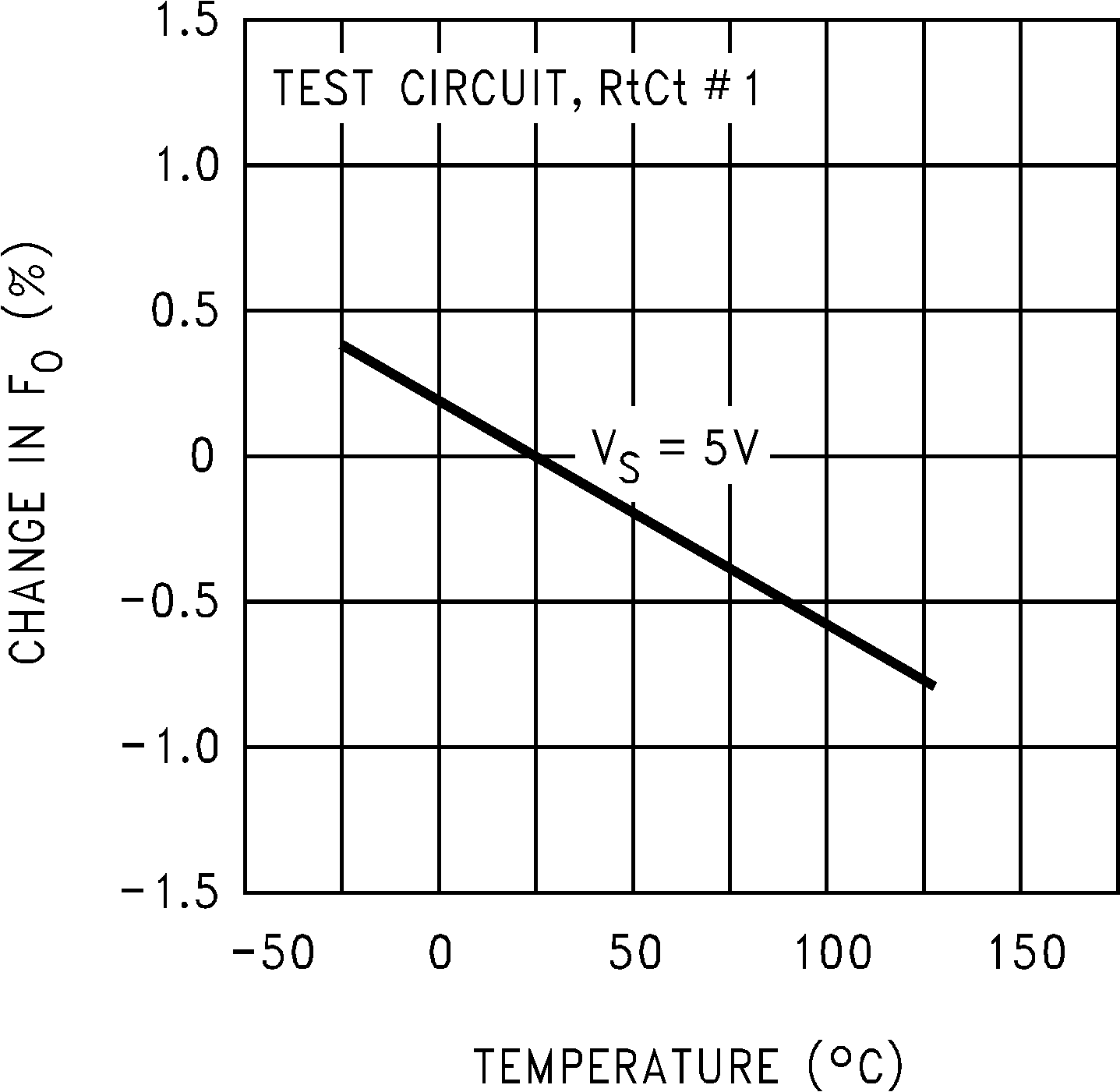 Figure 5. Frequency Drift With Temperature
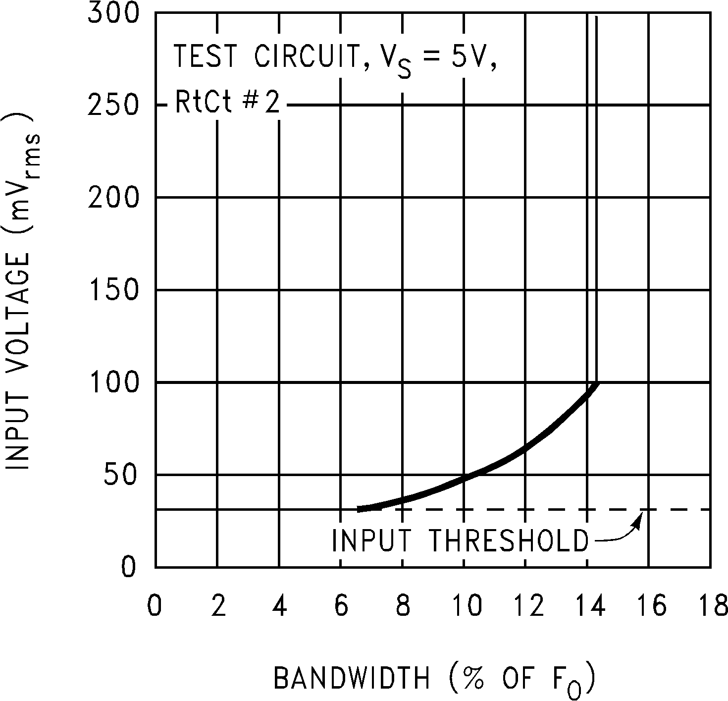 Figure 2. Bandwidth vs Input Signal Level
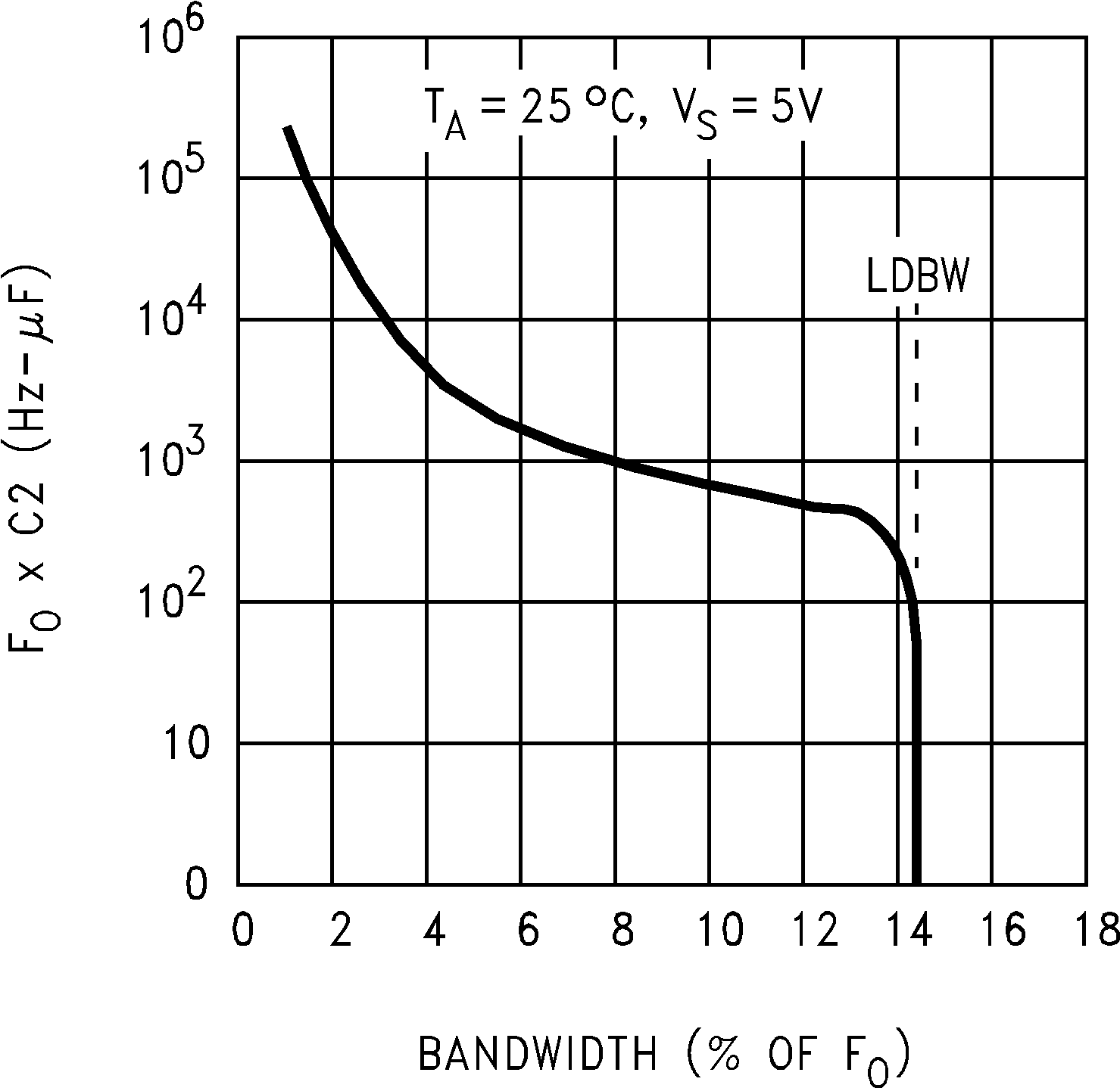 Figure 4. Bandwidth as a Function of C2
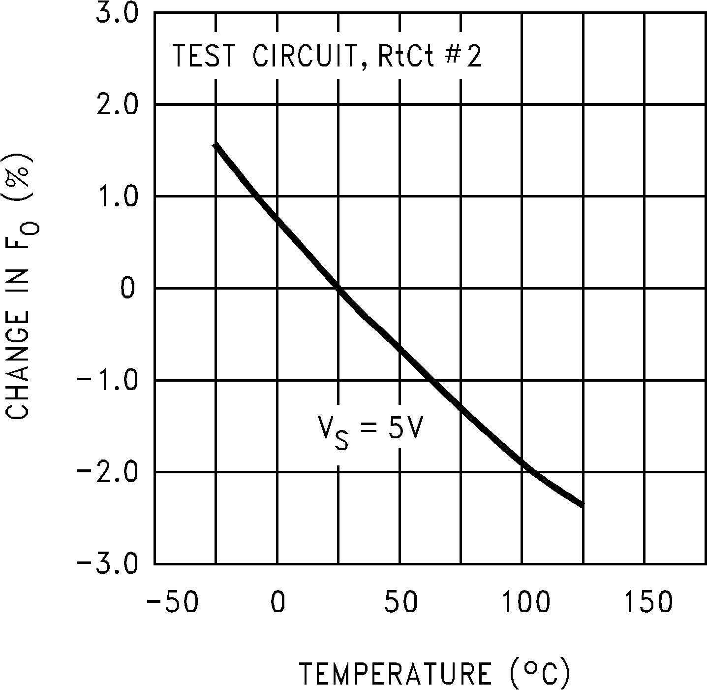 Figure 6. Frequency Drift With Temperature