SNOS738I April 1995 – January 2017 LM9061 , LM9061-Q1
PRODUCTION DATA.
- 1 Features
- 2 Applications
- 3 Description
- 4 Revision History
- 5 Pin Configuration and Functions
- 6 Specifications
- 7 Detailed Description
- 8 Application and Implementation
- 9 Power Supply Recommendations
- 10Layout
- 11Device and Documentation Support
- 12Mechanical, Packaging, and Orderable Information
8 Application and Implementation
NOTE
Information in the following applications sections is not part of the TI component specification, and TI does not warrant its accuracy or completeness. TI’s customers are responsible for determining suitability of components for their purposes. Customers should validate and test their design implementation to confirm system functionality.
8.1 Application Information
The LM9061 can be configured to drive the gate to any size external high-side power MOSFET, including multiple parallel connected MOSFETs for very high current applications. See Basic Operation for details on the gate drive operation and Turn On and Turn Off Characteristics for details on the gate drive timing characteristics.
8.2 Typical Applications
8.2.1 TITLE NEEDED
The LM9061 is an ideal driver for any application that requires multiple parallel MOSFETs to provide the necessary load current. Figure 19 shows a circuit with four parallel NDP706A MOSFETs. This circuit configuration provides a typical maximum load current of 150 A at 25°C, and a typical maximum load current of 100 A at 125°C.
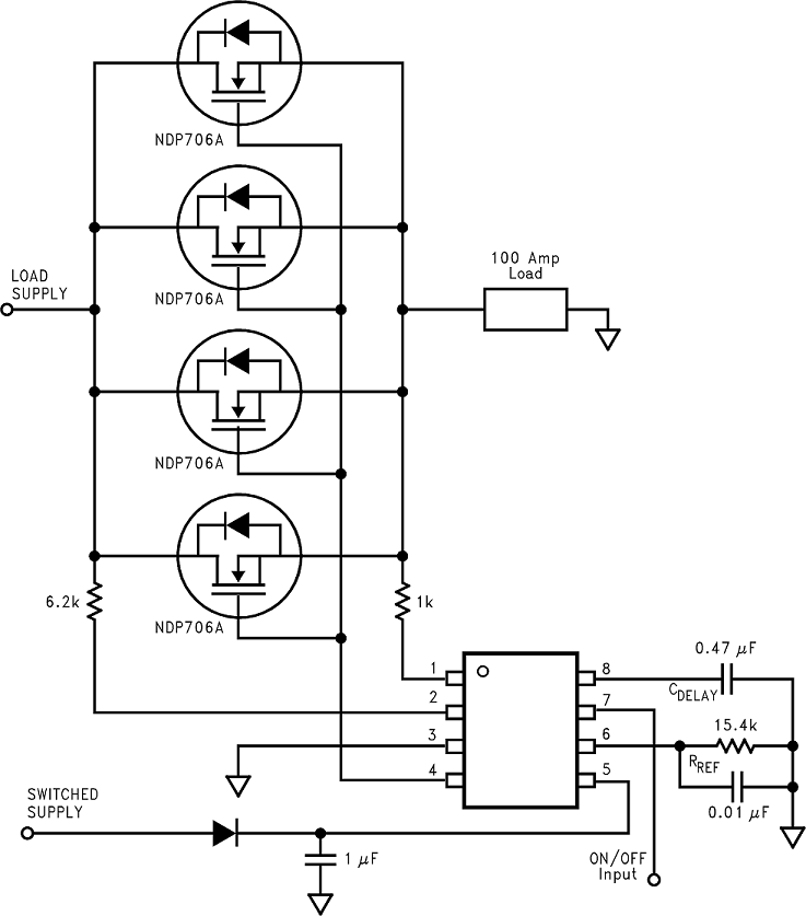 Figure 19. Driving Multiple MOSFETs
8.2.1.1 Design Requirements
Only a few common sense precautions need to be observed. All MOSFETs in the array must have identical electrical and thermal characteristics. This can be solved by using the same part number from the same manufacturer for all of the MOSFETs in the array. Also, all MOSFETs must have the same style heat sink or, ideally, all mounted on the same heat sink. The electrical connection of the MOSFETs should get special attention. With typical RDS(ON) values in the range of tens of mΩ, a poor electrical connection for one of the MOSFETs can render it useless in the circuit. Also, consider the MOSFET dissipation during the normal OFF discharge of the gate capacitance (70-µA minimum and 110-µA typical).
CAUTION
In the event of a fault condition, the Latch-OFF current sink, 10-µA typical, may not be able to discharge the total gate capacitance in a timely manner to prevent damage to the MOSFETs.
8.2.1.2 Detailed Design Procedure
The NDP706A MOSFET has a typical RDS(ON) of 0.013 Ω with a TJ of 25°C, and 0.02 Ω with a TJ of +125°C. An RTHRESHOLD value of 6.2 kΩ as shown in Figure 19 sets the VDS threshold voltage to approximately 500 mV. This provides a typical maximum load current of 150 A at 25°C, and a typical maximum load current of 100 A at 125°C. See Lossless Overcurrent Protection for details on calculating RTHRESHOLD.
The maximum dissipation, per MOSFET, is nearly 20 W at 25°C, and 12.5 W at 125°C. With up to 20 W being dissipated by each of the four devices, an effective heat sink is required to keep the TJ as low as possible when operating near the maximum load currents.
8.2.1.3 Application Curves
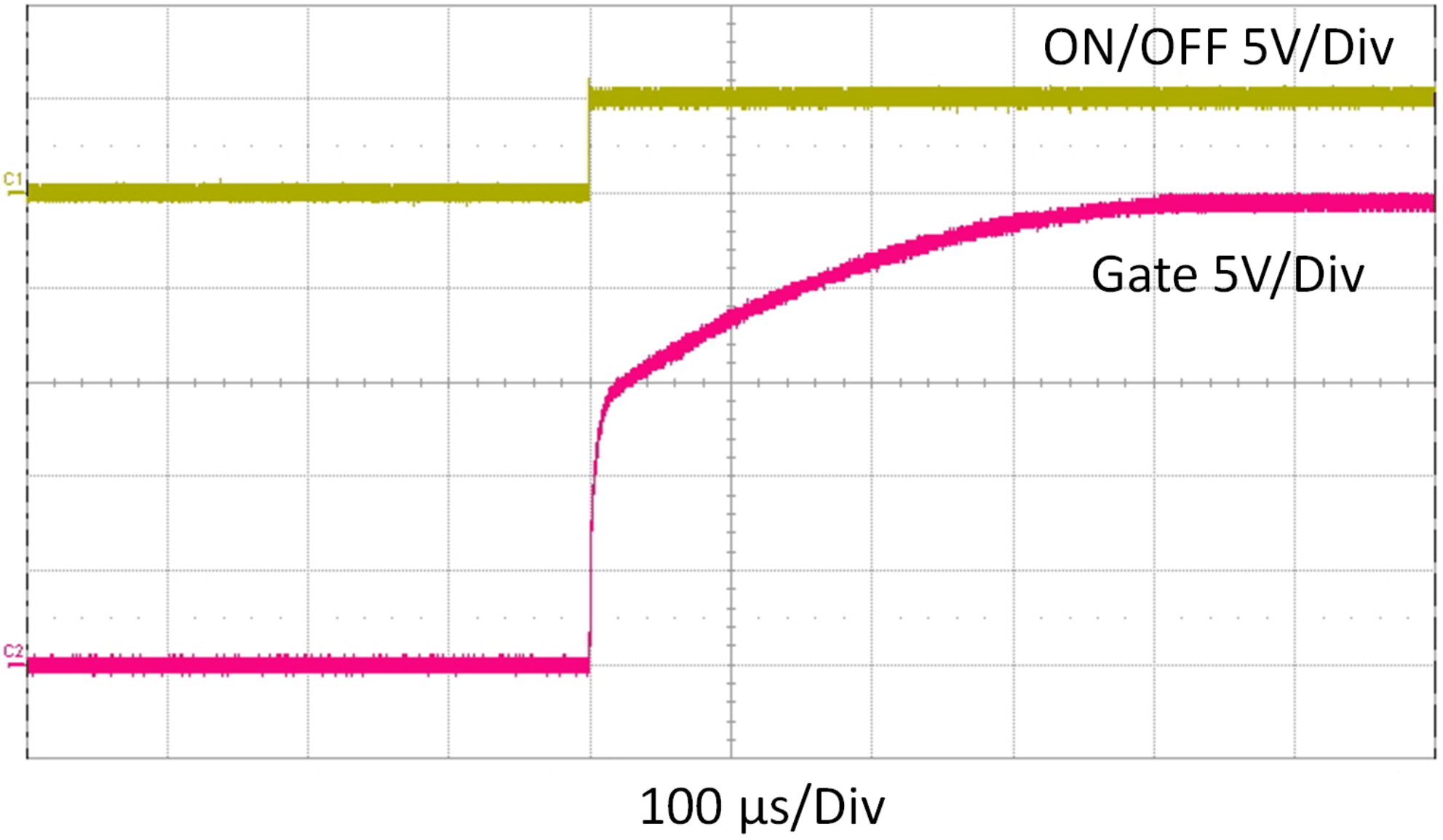 Figure 20. MOSFET Gate During Start-Up, Total Gate Capacitance = 11200 pF
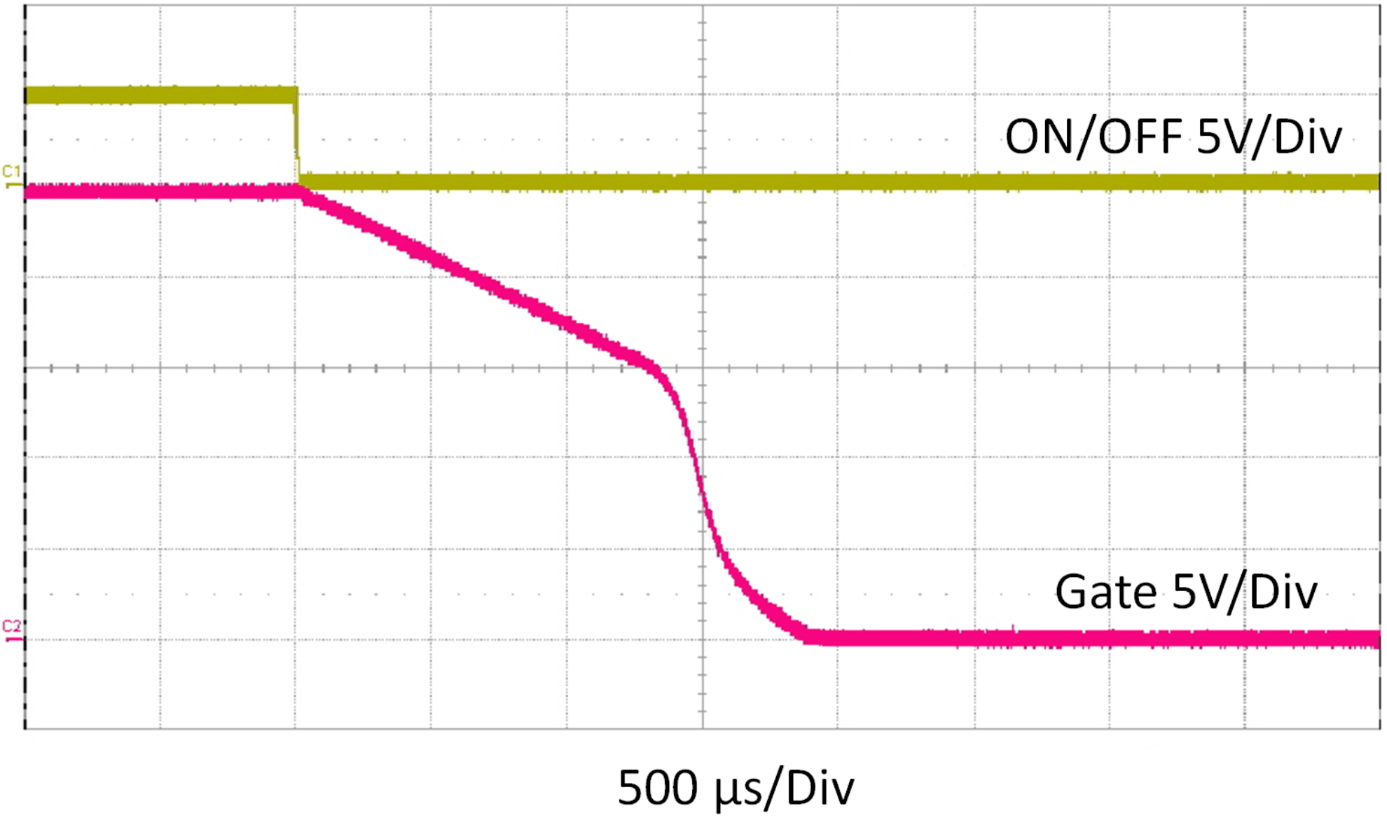 Figure 21. MOSFET Gate During Shutdown, Total Gate Capacitance = 11200 pF
8.2.2 Bidirectional Applications
8.2.2.1 Back-to-Back MOSFET Configuration
Due to the orientation of the FET, the typical configuration of LM9061 is only able to toggle conduction when current flows from the drain to the source. In applications where reverse current may occur, the body diode always provides a path from load to supply. For the LM9061’s OFF state to fully disconnect the load and supply and prevent any bidirectional current, an additional FET must be placed in series with the original. This back-to-back configuration shown in Figure 22 allows either input to be the supply side or the load side.
NOTE
An increase in turnon and turnoff time occurs due to the increased gate capacitance from the additional FET.
To provide the LM9061 with proper supply voltage, two diodes connect both inputs to VCC. This feeds the device with whichever side has a higher potential, ensuring that it does not disconnect itself from the voltage supply during operation.
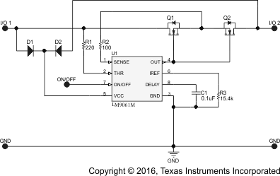 Figure 22. Bidirectional Switch
8.2.2.1.1 Application Curve
Here the bidirectional switch is being used to charge and discharge a capacitive load. As long as the switch is enabled ON, current is allowed to flow in and out of the capacitor in response to the steps in input voltage. However, when the switch is enabled OFF, current ceases to flow and the capacitor voltage is isolated from the input. Operation continues normally once the switch is returned to an ON state.
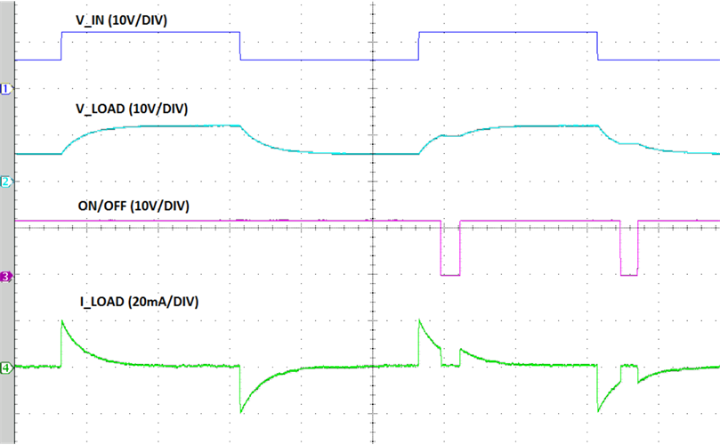 Figure 23. Bidirectional Switch Controlling Current to a Capacitive Load
8.2.2.2 Bidirectional Switch With Reverse Overcurrent Protection
While Figure 22 functions as a bidirectional switch, it does not monitor for overcurrent in both directions. Because overcurrent is detected when the potential at the sense pin is lower than the potential at the threshold pin by a user set amount, the LM9061 only offers OCP when the current flows through the FET before reaching the sense pin. To implement a bidirectional switch that also has bidirectional overcurrent protection, each FET should be controlled by its own LM9061 device. Figure 24 shows the two LM9061 and FET pairs in a mirrored back-to-back configuration. By tying the ON/OFF pins together, the switch can still be toggled from a single line.
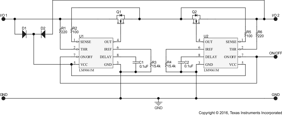 Figure 24. Bidirectional Switch Including Reverse OCP
8.2.2.2.1 Application Curve
The application curve below shows the reverse overcurrent protection. Even with the bidirectional current, the device goes into overcurrent shutdown if the current reaches the current limit threshold. Note that the reverse overcurrent protection is accomplished using two separate LM9061 devices as shown in Figure 24.
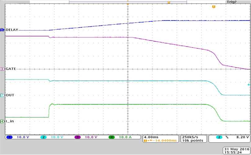 Figure 25. Reverse Overcurrent Protection for Bidirectional Switch