ZHCSNL2A February 2022 – May 2022 LM74502-Q1 , LM74502H-Q1
PRODUCTION DATA
- 1 特性
- 2 应用
- 3 说明
- 4 Revision History
- 5 Device Comparison Table
- 6 Pin Configuration and Functions
- 7 Specifications
- 8 Parameter Measurement Information
- 9 Detailed Description
-
10Application and Implementation
- 10.1 Application Information
- 10.2 Typical Application
- 10.3 Surge Stopper Using LM74502-Q1, LM74502H-Q1
- 10.4 Fast Turn-On and Turn-Off High Side Switch Driver Using LM74502H-Q1
- 11Power Supply Recommendations
- 12Layout
- 13Device and Documentation Support
- 14Mechanical, Packaging, and Orderable Information
10.4 Fast Turn-On and Turn-Off High Side Switch Driver Using LM74502H-Q1
In automotive load driving applications N-Channel MOSFET based high side switch is very commonly used to disconnect the loads from supply line in case of faults such as overvoltage event . LM74502-Q1, LM74502H-Q1 can be used to drive external MOSFET to realize simple high side switch with overvoltage protection. Figure 10-13 shows a typical application circuit where LM74502H-Q1 is used to drive external MOSFET Q1 as a main power path connect and disconnect switch. A resistor divider from input to OV pin to ground can be used the set the overvoltage threshold.
If VOUT node (SRC pin) of the device is expected to drop in case of events such as overcurrent or short-circuit on load side then additional Zener diode is required across gate and source pin of external MOSFET to protect it from exceeding its maximum VGS rating.
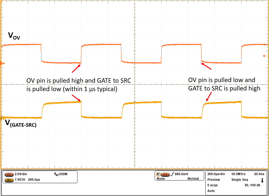
Many safety applications require fast switching off of the MOSFET in case of fault events such as overvoltage or overcurrent fault. Some of the load driving path applications also require PWM operation of high side switch. LM74502H-Q1 OV pin can be used as control input to realize fast turn-on and turn-off load switch functionality. With OV pin pulled above VOVR threshold of (1.25-V typical), LM74502H-Q1 turns off the external MOSFET (with Ciss = 4.7 nF) within 1 μs typically. When OV pin is pulled low, LM74502H-Q1 with its peak gate drive strength of 11 mA turns on external MOSFET with turn-on speed of 7-μs typical. Figure 10-14 shows LM74502H-Q1 GATE to SRC response when OV pin is toggled with ON/OFF logic input.
 Figure 10-14 Fast Turn-On and Turn-Off High Side Switch Driver Using LM74502H-Q1