ZHCSOA6A July 2021 – February 2022 LM74501-Q1
PRODUCTION DATA
- 1 特性
- 2 应用
- 3 说明
- 4 Revision History
- 5 Pin Configuration and Functions
- 6 Specifications
- 7 Parameter Measurement Information
- 8 Detailed Description
- 9 Application and Implementation
- 10Power Supply Recommendations
- 11Layout
- 12Device and Documentation Support
- 13Mechanical, Packaging, and Orderable Information
5 Pin Configuration and Functions
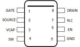
 Figure 5-1 DDF
Package8-Pin SOT-23(LM74501-Q1 Top View)
Figure 5-1 DDF
Package8-Pin SOT-23(LM74501-Q1 Top View)Table 5-1 LM74501-Q1 Pin Functions
| PIN | I/O(1) | DESCRIPTION | |
|---|---|---|---|
| NO. | NAME | ||
| 1 | GATE | O | Gate drive output. Connect to the gate of the external N-channel MOSFET. |
| 2 | SOURCE | I | Connect to the source of the external N-channel MOSFET. This pin also acts as the input supply for the device. |
| 3 | VCAP | O | Charge pump output. Connect to an external charge pump capacitor. |
| 4 | SW | I | Voltage sensing disconnect switch terminal. SOURCE and SW are internally connected through a switch when EN is high. A resistor ladder from this pin to GND can be used to monitor battery voltage. When EN is pulled low, the switch is OFF, disconnecting the resistor ladder from the battery line, thereby cutting off the leakage current. |
| 5 | GND | G | Ground pin |
| 6 | EN | I | Enable pin. Can be connected to SOURCE for always ON operation. |
| 7 | N.C | NA | No connect. Keep this pin floating. |
| 8 | DRAIN | I | Connect to the drain of the external N-channel MOSFET. |
(1) I = Input, O = Output, G = GND