SNVS234C September 2004 – September 2016 LM5112 , LM5112-Q1
PRODUCTION DATA.
10 Layout
10.1 Layout Guidelines
Attention must be given to board layout when using the LM5112 device. Some important considerations include:
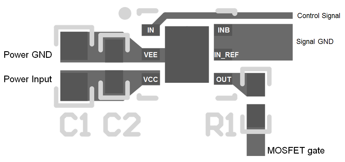
Proper grounding is crucial. The driver required a low impedance path for current return to ground avoiding inductive loops. Two paths for returning current to ground are a) between the LM5112 device IN_REF pin and the ground of the circuit that controls the driver inputs and b) between the LM5112 device VEE pin and the source of the power MOSFET being driven. Both paths must be as short as possible to reduce inductance and be as wide as possible to reduce resistance. These ground paths must be distinctly separate to avoid coupling between the high current output paths and the logic signals that drive the LM5112 device. With rise and fall times in the range of 10 nsec to 30 nsec, care is required to minimize the lengths of current carrying conductors to reduce their inductance and EMI from the high di/dt transients generated when driving large capacitive loads.
10.1.1 Thermal Considerations
The primary goal of the thermal management is to maintain the integrated circuit (IC) junction temperature (TJ) below a specified limit to ensure reliable long term operation. The maximum TJ of IC components must be estimated in worst case operating conditions. The junction temperature is calculated based on the power dissipated on the IC and the junction to ambient thermal resistance RθJA for the IC package in the application board and environment. The RθJA is not a given constant for the package and depends on the PCB design and the operating environment.
10.1.1.1 Drive Power Requirement Calculations In LM5112
The LM5112 device is a single, low-side MOSFET driver capable of sourcing and sinking 3-A or 7-A peak currents for short intervals to drive a MOSFET without exceeding package power dissipation limits. High peak currents are required to switch the MOSFET gate quickly for operation at high frequencies.
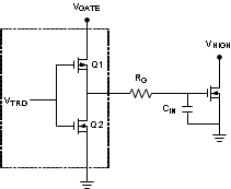
 Figure 18. MOSFET Driver Diagram
Figure 18 shows a conceptual diagram of the LM5112 device output and MOSFET load. Q1 and Q2 are the switches within the gate driver. RG is the gate resistance of the external MOSFET, and Cin is the equivalent gate capacitance of the MOSFET. The equivalent gate capacitance is a difficult parameter to measure as it is the combination of CGD (gate to source capacitance) and CGD (gate to drain capacitance). The CGD is not a constant and varies with the drain voltage. The better way of quantifying gate capacitance is the gate charge QG in coloumbs. QG combines the charge required by CGD and CGD for a given gate drive voltage VGATE. The gate resistance RG is usually small and losses in it are neglected. The total power dissipated in the MOSFET driver due to gate charge is approximated by Equation 1.
where
- FSW = switching frequency of the MOSFET
For example, consider the MOSFET MTD6N15 whose gate charge specified as 30 nC for VGATE = 12 V.
Therefore, the power dissipation in the driver due to charging and discharging of MOSFET gate capacitances at switching frequency of 300 kHz and VGATE of 12 V is equal to Equation 2.
In addition to the above gate charge power dissipation, - transient power is dissipated in the driver during output transitions. When either output of the LM5112 device changes state, current flows from VCC to VEE for a brief interval of time through the output totem-pole N and P channel MOSFETs. The final component of power dissipation in the driver is the power associated with the quiescent bias current consumed by the driver input stage and Undervoltage lockout sections.
Characterization of the LM5112 device provides accurate estimates of the transient and quiescent power dissipation components. At 300 kHz switching frequency and 30 nC load used in the example, the transient power is 8 mW. The 1 mA nominal quiescent current and 12 V VGATE supply produce a 12 mW typical quiescent power.
Therefore, the total power dissipation is calculated with Equation 3.
The junction temperature is given by Equation 4.
Or the rise in temperature is given by Equation 5.
For 6-pin WSON package, the integrated circuit die is attached to leadframe die pad which is soldered directly to the printed circuit board. This substantially decreases the junction to ambient thermal resistance (RθJA). By providing suitable means of heat dispersion from the IC to the ambient through exposed copper pad, which can readily dissipate heat to the surroundings, RθJA as low as 40°C/W is achievable with the package. The resulting TRISE for the driver example above is thereby reduced to just 5.5°C.
Therefore, TRISE is equal to Equation 6.
For MSOP-PowerPAD, RθJA is typically 60°C/W.
10.2 Layout Example
 Figure 19. LM5112 Layout Example