ZHCSNW4 October 2022 LM5012-Q1
PRODUCTION DATA
- 1 特性
- 2 应用
- 3 说明
- 4 Revision History
- 5 Device Comparison Table
- 6 Pin Configuration and Functions
- 7 Specifications
-
8 Detailed Description
- 8.1 Overview
- 8.2 Functional Block Diagram
- 8.3
Feature Description
- 8.3.1 Control Architecture
- 8.3.2 Internal VCC Regulator and Bootstrap Capacitor
- 8.3.3 Regulation Comparator
- 8.3.4 Internal Soft Start
- 8.3.5 On-Time Generator
- 8.3.6 Current Limit
- 8.3.7 N-Channel Buck Switch and Driver
- 8.3.8 Schottky Diode Selection
- 8.3.9 Enable/Undervoltage Lockout (EN/UVLO)
- 8.3.10 Power Good (PGOOD)
- 8.3.11 Thermal Protection
- 8.4 Device Functional Modes
- 9 Application and Implementation
- 10Device and Documentation Support
- 11Mechanical, Packaging, and Orderable Information
8.3.1 Control Architecture
The LM5012 step-down switching converter employs a constant on-time (COT) control scheme. The COT control scheme sets a fixed on time, tON, of the high-side FET using a timing resistor (RON). tON is adjusted as VIN changes and is inversely proportional to the input voltage to maintain a fixed frequency when in continuous conduction mode (CCM). After tON expires, the high-side FET remains off until the feedback pin is equal or below the 1.2-V reference voltage. To maintain stability, the feedback comparator requires a minimal ripple voltage that is in-phase with the inductor current during the off time. Furthermore, this change in feedback voltage during the off time must be large enough to dominate any noise present at the feedback node. The minimum recommended feedback ripple voltage is 20 mV. See Table 8-1 for different types of ripple injection schemes that ensure stability over the full input voltage range.
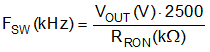
During a rapid start-up or a positive load step, the regulator operates with minimum off times until regulation is achieved. This feature enables extremely fast load transient response with minimum output voltage undershoot. When regulating the output in steady-state operation, the off time automatically adjusts itself to produce the SW-pin duty cycle required for output voltage regulation to maintain a fixed switching frequency. In CCM, the switching frequency, FSW, is programmed by the RRON resistor. Use Equation 2 to calculate the switching frequency.
| Type 1 | Type 2 | Type 3 |
|---|---|---|
| Lowest Cost | Reduced Ripple | Minimum Ripple |
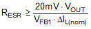 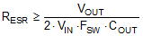 |  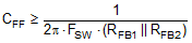 | 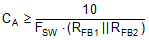 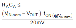 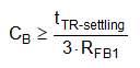 |
Table 8-1 presents three different methods for generating appropriate voltage ripple at the feedback node. Type-1 ripple generation method uses a single resistor, RESR, in series with the output capacitor. The generated voltage ripple has two components: capacitive ripple caused by the inductor ripple current charging and discharging the output capacitor and resistive ripple caused by the inductor ripple current flowing into the output capacitor and through series resistance, RESR. The capacitive ripple component is out-of-phase with the inductor current and does not decrease monotonically during the off time. The resistive ripple component is in-phase with the inductor current and decreases monotonically during the off time. The resistive ripple must exceed the capacitive ripple at VOUT for stable operation. If this condition is not satisfied, unstable switching behavior is observed in COT converters with multiple on-time bursts in close succession followed by a long off time. The lowest cost bill of materials (BOM) define the value of the series resistance RESR to ensure sufficient in-phase ripple at the feedback node.
Type-2 ripple generation uses a CFF capacitor in addition to the series resistor. As the output voltage ripple is directly AC-coupled by CFF to the feedback node, the RESR and ultimately the output voltage ripple, are reduced by a factor of VOUT / VFB1.
Type-3 ripple generation uses an RC network consisting of RA and CA, and the switch node voltage to generate a triangular ramp that is in-phase with the inductor current. This triangular wave is the AC-coupled into the feedback node with capacitor CB. Because this circuit does not use output voltage ripple, it is suited for applications where low output voltage ripple is critical. The Selecting an Ideal Ripple Generation Network for Your COT Buck Converter application report provides additional details on this topic.